Board Specific Specifications and Information
This page contains specification and architecture information for the AMD Embedded Development Framework (EDF) that is applicable to specific evaluation boards, including pinout, interfaces, and memory map implementation.
Introduction
Evaluation board specific information can be found in the following sections. The information is organized by device/device family, and then by evaluation board using the board name.
VEK385
Boot Firmware and Linux Disk Images
Boot Firmware Images - OSPI VEK385 - Boot Firmware + boot.pdi:
Refer to Common Specifications
Linux Disk Image - Common Disk Image With Support for This Board
Refer to Common Specifications
Boot Flow - Arm System Ready Compatible Boot Flow With UEFI
AMD EDF v26.06 (VEK385) - AMD Vivado Design Suite 2026.1
OSPI Memory Map - 2G Micron Device (VEK280, VEK385)
For the Micron 2b OSPI device memory device MT35XLU02G part used on VEK280, VEK385 evaluation boards. See Common Specifications for more information.
This part has the same erasable and lockable sector size of 128 KB, which defines the minimum footprint for each section within the OSPI memory map. The overall map is described in the table below and is aligned to the 1 Gb for the “fixed” section. It can facilitate user application space for A/B images, and is pre-allocated for 114 MB to accommodate the larger device targets.
Start Address |
Description |
Size (KB) |
Start Sector |
R or R/W |
MTD |
MultiBoot Offset |
|---|---|---|---|---|---|---|
0x0000 0000 |
Image Selector App |
384 |
0 |
R |
0 |
0x0000 |
0x0006 0000 |
Image Selector App - Backup |
384 |
3 |
R |
1 |
0x000C |
0x000C 0000 |
Image Selector - Scratchpad |
128 |
6 |
R |
2 |
|
0x000E 0000 |
Image Recovery App |
20480 |
7 |
R |
3 |
0x001C |
0x014E 0000 |
Image Recovery - Scratchpad |
128 |
167 |
R |
4 |
|
0x0150 0000 |
SystemReady-DT Update Metadata |
128 |
168 |
R/W |
5 |
|
0x0152 0000 |
SystemReady-DT Update Metadata (Backup) |
128 |
169 |
R/W |
6 |
|
0x0154 0000 |
U-Boot Variables |
128 |
170 |
R/W |
7 |
|
0x0156 0000 |
U-Boot Variables (Backup) |
128 |
171 |
R/W |
8 |
|
0x0158 0000 |
Bank “A” Image Space / Directory |
116736 |
172 |
R/W |
9 |
0x02B0 |
0x0878 0000 |
U-Boot Variables - Bank A - Design option |
128 |
1084 |
R/W |
10 |
|
0x087A 0000 |
U-Boot Variables - Bank A (Backup) |
128 |
1085 |
R/W |
11 |
|
0x087C 0000 |
Bank “B” Image Space / Directory |
51200 |
1086 |
R/W |
12 |
0x10F8 |
0x0F9C 0000 |
U-Boot Variables - Bank B - Design option |
128 |
1998 |
R/W |
13 |
|
0x0F9E 0000 |
U-Boot Variables - Bank B (Backup) |
128 |
1999 |
R/W |
14 |
|
0x0FA0 0000 |
User Scratchpad |
6016 |
2000 |
R/W |
15 |
DDR Memory Map - VEK385
The VEK385 Memory Map is based on the AMD EDF System Memory map standard Common Specifications The following table represents the VEK385 specific map, reflecting the number of RPUs and physical memory available in the platform.
Start Addr |
Size (MB) |
Description |
Fixed/Variable |
XMPU |
|---|---|---|---|---|
Low DDR - 2 GB |
||||
0x000 0000 0000 |
16 |
Versal PLM |
Fixed |
Yes - PLM FW |
0x000 0100 0000 |
6 |
TF-A - Transfer list / handoffs |
Fixed |
TBD |
0x000 0160 0000 |
2 |
TF-A - Core runtime memory |
Fixed |
Yes - TF-A FW |
0x000 0180 0000 |
128 |
OP-TEE shared buffers & dynamic TAs |
Fixed |
Yes - Secure OS/Secure Partition |
0x000 0980 0000 |
8 |
RPU Core 0-1 OpenAMP allocations (4 MB / core) |
x2 RPU Cores |
Yes - RPU |
32 |
Free memory |
|||
0x000 0C00 0000 |
320 (400 MB requested) |
RPU+:term:ISP reservation |
x3 ISP |
Yes - RPU |
0x000 2000 0000 |
1536 |
Linux - Low DDR |
LOW_DDR Remainder |
No |
High DDR |
||||
0x008 0000 0000 |
2048 |
ISP frame buffer allocation (DDRMC closest to ISPs) |
Scale # ISPs |
|
Platform dependent |
Linux - High DDR |
HIGH_DDR Remainder |
||
Platform dependent |
PL & AIE dedicated allocations |
Programing/flashing the OSPI (Primary Boot Device)
See
Programing the UFS / SD Card(Secondary Boot device)
The secondary boot device on the VEK385 depends on the board revision:
VEK385 Rev A uses an SD card as the secondary boot device. Rev A boards do not support UFS.
VEK385 Rev B uses a UFS device as the secondary boot device. UFS is only supported on Rev B.
For other Versal boards (for example, VEK280 and VCK190), use an SD card as the secondary boot device.
For step-by-step procedures for writing the disk image to either media, see:
Writing the EDF Linux Disk Images (wic) to the Secondary Boot Media: SD Card (VEK385 Rev A, VEK280, VCK190)
Writing the EDF Linux Disk Images (wic) to the Secondary Boot Media: UFS device (VEK385 Rev B only)
VEK385 Basic Board Interfaces
The following picture shows the location of the basic board interfaces. For more information, see the Evaluation board user guide.
The basic board setup is as follows:
Connect the external power supply to the “Power Connector” (J28)
Connect the USB-Type C connector (J26) labeled “USB Type-C JTAG/UART” to the host PC
Connect the RJ45 (J52) labeled “PS Ethernet” to the local network
Connect the RJ45 (J64) labeled “SC Ethernet” (System Controller) to the local network
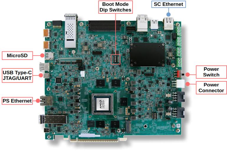
VEK385 board with key interfaces annotated.
VEK385 Powering the Board
To power up the board, connect the board external power supply to an outlet, plug in the external supply to the VEK385 board and turn the board on with the power switch:
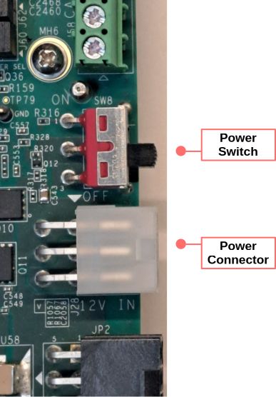
VEK385 Power Switch and Power Connector.
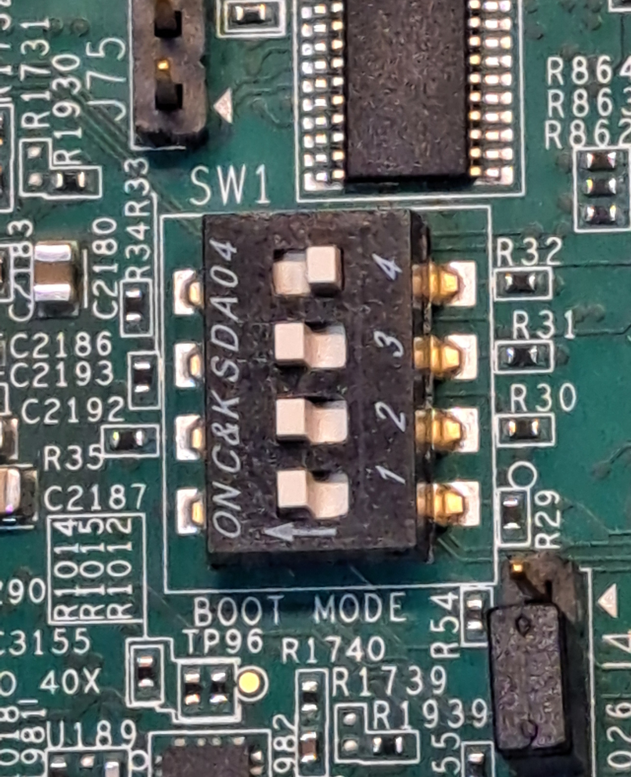
VEK385 Default DIP Switch Settings - Boot
System Controller Firmware Update
See the System Controller Wiki for more information https://xilinx-wiki.atlassian.net/wiki/x/AYCGhw
VEK385 UART connections - FTDI-USB
The VEK385 has four serial / UART interfaces. When the FTDI-USB cable is plugged into the VEK385 board it creates four device nodes on the host PC.
The four UART are mapped as follows,
Rev B:
FDTI |
DUT (2VE3858) |
|
|---|---|---|
ADBUS (Device 0) |
||
BDBUS (Device 1) |
PS-UART0 |
PS-UART1 |
NC |
||
PS-UART0 |
||
PS-UART1 |
NC |
Rev A:
FDTI |
DUT (2VE3858) |
|
|---|---|---|
ADBUS (Device 0) |
||
BDBUS (Device 1) |
PS-UART0 |
PS-UART1 |
NC |
PS-UART0 |
|
PS-UART1 |
NC |
FTDI - System Controller - Versal; UART diagram Rev B
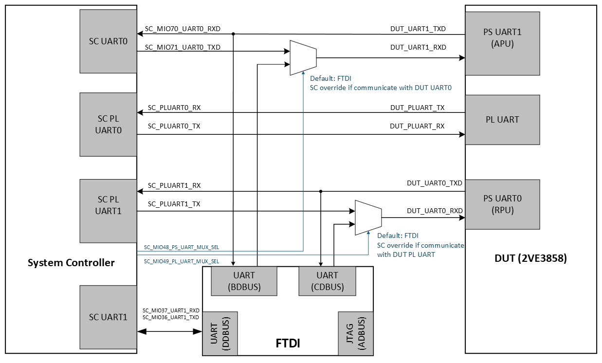
VEK385 Rev B FTDI / System Controller / Versal UART routing.
Rev A
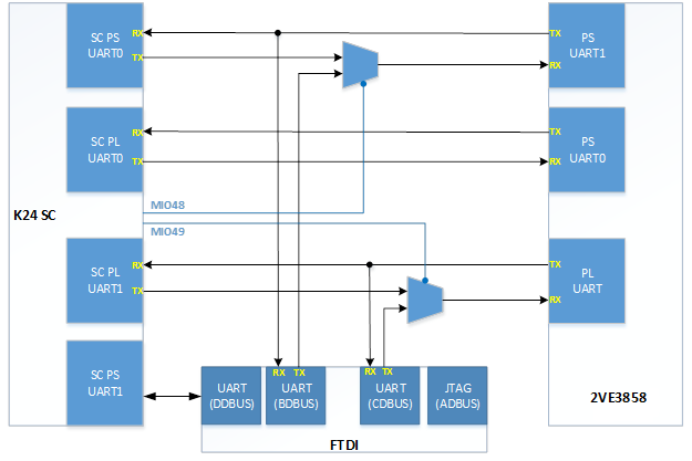
VEK385 Rev A FTDI / System Controller / Versal UART routing.
Versal PS-UART1 is used by the primary user software (U-Boot and Linux). This can be directly accessed by the host PC through the FTDI UART.
Versal PS-UART0 is used by default for auxiliary software (PLM, ASU, RPU) and on Rev A boards is routed to the System Controller for remote UART functionality. In Rev B of the VEK385, PS-UART0 is directly accessible through the FTDI-USB interface. It is a known limitation in this configuration that PLM power-on messages are not accessible in this VEK385 Rev A configuration. The users can work around this by issuing a Versal POR_B and capturing logs from the System Controller.
VEK385 Base Vivado Design for BSPs and PS specifications
This specification inherits from the common and device specific specifications, but also has evaluation board specific items. See also the following:
The Versal Gen 2 AI Edge Series Gen 2 Embedded Common Platform CED from AMD Vivado Design Suite 2026.1 is the base Vivado design used for EDF BSPs.
it is the recommended starting point for Vivado designs to maintain compatibility with the prebuilt OSPI boot images, and EDF prebuilt disk images.
VEK385 PL Board I/O
The Base CED PL design includes AXI-GPIO controllers that must be used of the “GPIO” physical interfaces for customer test. These are summarized in the following table. They are split across unique controllers to align with mapping to Vivado Board File signal groups and to minimize customer confusion on bitwise definitions.
Controller |
Description |
Location |
PL IP Direction |
|---|---|---|---|
PL_AXI_GPIO_0 |
GPIO_LED[3:0] |
Bank 705 & 706 |
Output |
PL_AXI_GPIO_1 |
GPIO_PB[1:0] |
Bank 705 & 706 |
Input |
PL_AXI_GPIO_2 |
GPIO_DIP[3:0] |
Bank 705 & 706 |
Input |
VEK385 MMI Configuration
The MMI configuration for VEK385 is aligned with the VEK385 hardware design. This includes the following configurations:
Base Configuration
PCIe 10GbE HSDP GT = PCIe0 x2 10GbE
USB DisplayPort GT = DP X2 + USB
USB Configuration
USB3.2 = Enabled
USB2.0 = Enabled (automatic with 3.2 enable)
10GbE Configuration
Data Rate = 10G
MDIO = Not enabled / None
External FIFO = Not enabled
External TSU Interface = Not enabled
PTP Interface = Not enabled
DPDC Configuration
Operating Mode = DC Functional
Presentation Mode = Non Live
Video Interface Mode = Native
DP Hot Plug Detect = PMC MIO 48
MMI PCIe Controller 0
Link
Port Type = Root Port of PCIe Root Port Complex
Link Speed = 32 GT/s
Mode = TBD
PERST = None (Handled by SW)
PF Basic, PF BARs, SRIOV - N/A as in Root Port mode
VEK385 MMI Clocks:
Video Clocks - Derived off a common MBUFGCE
MMI 2x Clk = 600 MHz
MMI 1x Clk = 300 MHz
Audio Clock
192kHz x 512 = 98.304 MHz
Dynamic Config = Must be enabled so the DP driver can adjust frequencies based on display resolution.
VEK385 Reference PL Payload Information
See the Discovery and Evaluation
ZCU104
Default Boot Flow
The default boot flow for the EDF Linux BSP for ZCU104 is Common Specifications
See Common Specifications for more information.
ZCU104 Boot Firmware and Linux Disk Images
Boot Firmware Images
Not applicable
Linux Disk Image - Common Disk Image With Support for This Board
edf-linux-disk-image-amd-cortexa53-mali-common+zynqmp-zcu104-sdt-full.rootfs.wic.xz
Advanced Embedded Software Configurations Included
Xen Dom0 (through
edf-platform-disk-image; see image-variant comparison)OpenAMP runtime packages (through
edf-platform-disk-image); per-board firmware example tarballs to follow in EDF 26.1.1xen-zephyr-domu-imageZephyr DomU payload to follow in EDF 26.2
ZCU104 UART connections - FTDI-USB
The ZCU104 board uses the quad USB-UART chip, that enables four UART interfaces through a single micro-AB USB connector:
ZCU104 Ethernet connections
The ZCU104 board physically uses GEM3 for its Ethernet interface.
ZCU104 base design (CED) and PS specifications
The AMD Vivado design suite project used for the ZCU104 EDF BSP inherits the aims of the common specifications in EDF. The design is created using board automation within Vivado, with additional Tcl scripting. However, there is minimal direct inheritance from the documented common specifications which are AMD Versal device portfolio based.
Refer to the board specific configurations here, which are migrated to Device Specific Specifications as and when additional boards are added.
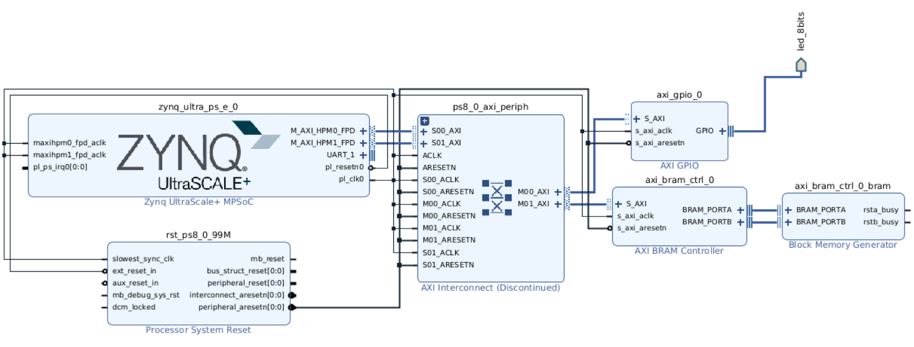
The AMD Vivado design suite projects used for the ZCU104 EDF BSP are:
zcu104_basewhich can be downloaded from zcu104_basezcu104_pl_vcu_extensiblewhich can be downloaded from zcu104_pl_vcu_extensible
A picture of the block design generated including PL content is shown below:
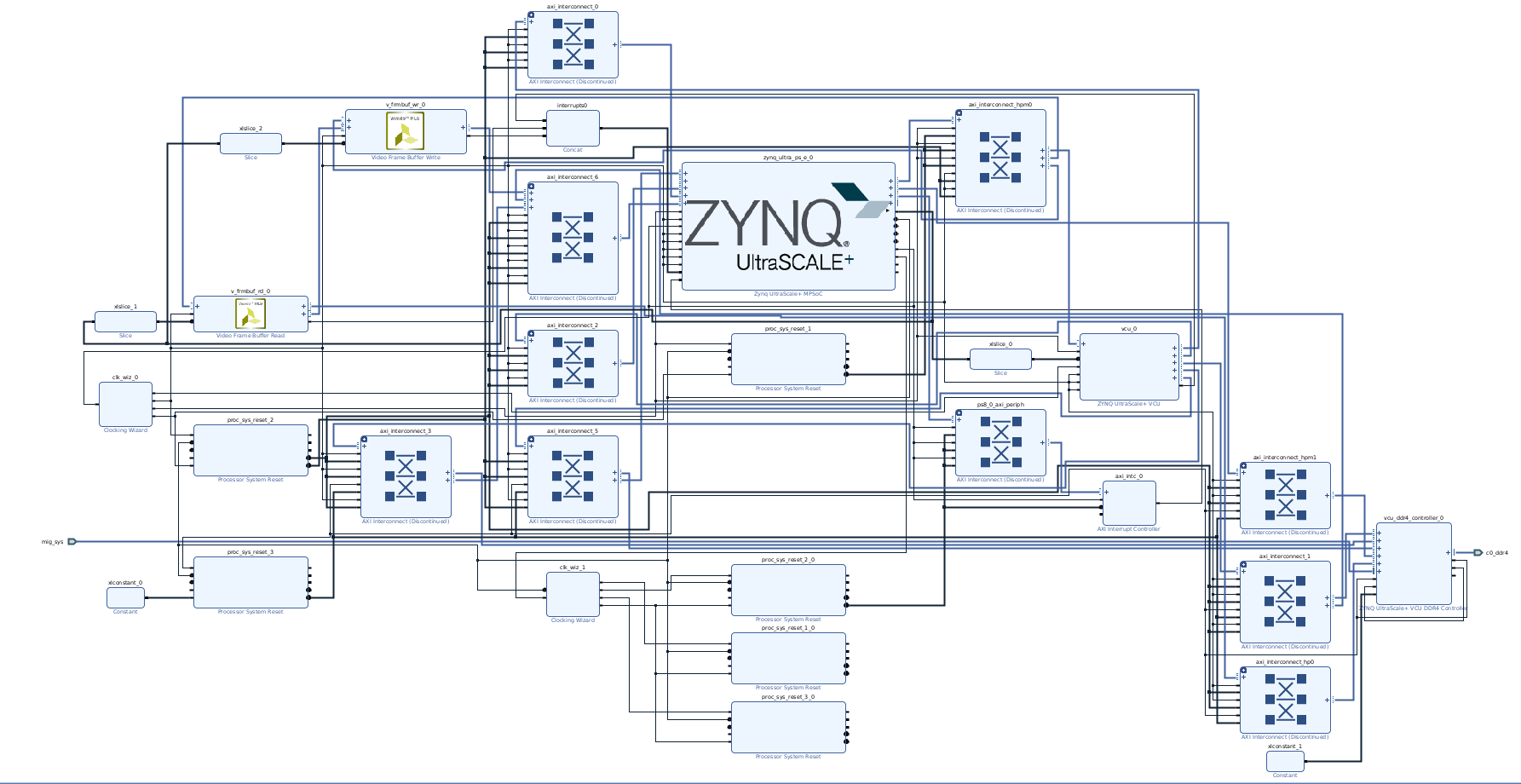
PL Payload:
Default Payload: - VCU Extensible Platform
AXI-V_FRMBUF_WR
Transfers video pixel data into memory.
AXI-VCU
Encodes and decodes video streams.
AXI-VCU_DDR4_CONTROLLER
Interfaces with DDR4 memory for high-speed video data access.
Additional Payloads:
PS Specifications:
The following default PS configuration is implemented in the embedded common platform CED for Zynq Ultrascale+, and is aligned with common specifications, there are also some board defined items such as fixed MIO, clocks, and enabling clock frequencies enabled by the speed grade of the target device.
PS Peripheral mappings in the CED
CAN1: Mapped to MIO pins 24 and 25.
DisplayPort AUX Channel: Mapped to MIO pins 27 to 30.
ENET3 MDIO: Mapped to MIO pins 76 and 77.
ENET3 data and control signals: Mapped to MIO pins 64 to 75.
GPIO: Assigned to EMIO interface with 92 signals.
I2C1: Mapped to MIO pins 16 and 17.
SD1: Mapped to MIO pins 46 to 51.
TTC0, TTC1, TTC2, TTC3: Assigned to EMIO interface.
UART0: Mapped to MIO pins 18 and 19.
UART1: Mapped to MIO pins 20 and 21.
Interrupts
PS-PL Interrupts
The embedded common platform CED enables two LPD interrupts.
The following table outlines the planned application mapping and utilization of the PS-PL interrupts.
Domain |
IRQ |
Enabled |
Allocation |
|---|---|---|---|
1 |
Yes |
PL Interrupts |
|
9 |
Yes |
PL Interrupts |
IPI Mappings
The embedded common platform CED enables a superset of IPI mappings to support current and future TRDs and are defined in the following table.
These do not impact the PS/PL boundary so are not controlled relative to TRD specific PL designs.
IPI / IRQ |
Enabled |
Master |
Description |
|---|---|---|---|
axi_intc_0 |
Yes |
zynq_ultra_ps_e_0 |
AXI Interrupt Controller (aggregates PL interrupts) |
pl_ps_irq0 |
Yes |
zynq_ultra_ps_e_0 |
|
pl_ps_irq1 |
Yes |
zynq_ultra_ps_e_0 |
DDR Memory Map
The following represents the map reflecting the number of RPUs and physical memory available in the platform.
Region Name |
Start Address |
Size (Bytes) |
Description |
|---|---|---|---|
Main DDR Region |
0x00000000 |
0x80000000 (2 GB) |
Primary DDR accessed through HPx ports (APU/Linux) |
VCU Decode Buffer |
0x4800000000 |
0x80000000 (2 GB) |
VCU decode data through S_AXI_PORT0 |
VCU Encode Buffer |
0x4800000000 |
0x80000000 (2 GB) |
VCU encode data through S_AXI_PORT1 |
VCU Code/Data Region |
0x4800000000 |
0x80000000 (2 GB) |
VCU code buffer through S_AXI_PORT2 |
Framebuffer Read Region |
0x4800000000 |
0x80000000 (2 GB) |
Framebuffer read through S_AXI_PORT4 |
VCU Frame Buffer |
0x4800000000 |
0x80000000 (2 GB) |
VCU frame buffer through S_AXI_PORT3 |
System Level Memory Map
The system level memory map shown here focuses on the DDR, OCM, and TCM allocations within the AMD EDF architecture.
The following table defines the default allocations used by AMD EDF, and what AMD reference designs use as their starting points. Due to the nature of device tree definition, end users can change this.
Start Address |
Description |
|---|---|
0x80000000 |
|
0xA0000000 |
Framebuffer Control Read/Write |
0xA0010000 |
VCU S_AXI_LITE |
0x4800000000 |
DDR Controller S_AXI_PORT3 |
0x4800000000 |
DDR Controller S_AXI_PORT4 |
0xC0000000 |
QSPI Linear (HPx_QSPI) |
0xFF000000 |
HPx_LPS_OCM |
0x00000000 |
HPx_DDR_LOW (Main DDR) |
0x4800000000 |
VCU Code/Data/Enc/Dec Buffers |
ZCU111
Default Boot Flow
The default boot flow for the EDF Linux BSP for ZCU111 is Common Specifications
See Common Specifications for more information.
ZCU111 Boot Firmware and Linux Disk Images
Boot Firmware Images
Not applicable
Linux Disk Image - Common Disk Image With Support for This Board
edf-linux-disk-image-amd-cortexa53-common+zynqmp-zcu111-sdt-full.rootfs.wic.xz
Advanced Embedded Software Configurations Included
Xen Dom0 (through
edf-platform-disk-image; see image-variant comparison)OpenAMP runtime packages (through
edf-platform-disk-image); per-board firmware example tarballs to follow in EDF 26.1.1xen-zephyr-domu-imageZephyr DomU payload to follow in EDF 26.2
ZCU111 UART connections - FTDI-USB
The ZCU111 board uses the quad USB-UART chip, that enables four UART interfaces through a single micro-AB USB connector:
ZCU111 Ethernet connections
While the ZCU111 board physically uses GEM3 for its Ethernet interface.
ZCU111 base design (CED) and PS specifications
The AMD Vivado design suite project used for the ZCU111 EDF BSP
is: zcu111_base which can be downloaded from
zcu111_base
A picture of the block design generated including PL content is shown below:
ZCU111 base block design.
PL Payload - EDF minimal PL Payload
PL Payload Content
Additional Payloads
EDF v26.06 - None
PS Specifications
The following default PS configuration is implemented in the embedded common platform CED for Zynq UltraScale+, and is aligned with common specifications, there are also some board defined items such as fixed MIO, clocks, and enabling clock frequencies enabled by the speed grade of the target device.
PS Peripheral mappings in the CED
MIO Controller — All MIO controllers (for example, UART, I2C, SPI) associated with fixed PS peripherals are enabled and configured based on the board design.
MIO I/O Configuration — MIO pins are configured based on the platform hardware setup, including drive strength, slew rate, and pull-up/down settings.
UART1 — Enabled for console communication; mapped through MIO pins to provide serial access during boot and runtime.
AXI HP Interfaces (HPM0_FPD, HPM1_FPD) — Configured so the PS can access PL-connected peripherals like BRAM, GPIO, and Interconnect through high-performance AXI master ports.
Interrupts
IPI Mappings
The embedded common platform CED enables a superset of IPI mappings to support current and future TRDs and are defined in the following table.
These do not impact the PS/PL boundary so are not controlled relative to TRD specific PL designs.
IPI |
Enabled |
Master |
Description |
|---|---|---|---|
IPI 0 |
Yes |
Inter-core messaging (for example, APU0 ↔ PMU) |
|
IPI 1 |
Yes |
RPU0 |
Real-time processor messaging |
IPI 2 |
Yes |
RPU1 |
Real-time processor messaging |
IPI 3 |
Yes |
||
Yes |
Platform management functions |
||
Yes |
Platform management functions (bufferless) |
||
Yes |
Security management functions |
DDR Memory Map
The following represents the map reflecting the number of RPUs and physical memory available in the platform.
Start Address |
End Address |
Size (MB) |
Description |
|---|---|---|---|
0x00000000 |
0x3ECFFFFF |
~1003 |
Usable DDR (Linux, apps, heap) |
0x3ED00000 |
0x3EDFFFFF |
1 |
Reserved for RPU / OpenAMP |
0x3EE00000 |
0x3FFFFFFF |
~19 |
Usable DDR continues |
0xFD070000 |
0xFD09FFFF |
0.1875 (~192 KB) |
DDR Controller (registers only) |
System Level Memory Map
The system level memory map shown here focuses on the DDR, OCM, and TCM allocations within the AMD EDF architecture.
The following table defines the default allocations used by AMD EDF, and what AMD reference designs use as their starting points. Due to the nature of device tree definition, end users can change this.
Start Address |
Description |
|---|---|
0x00000000 |
DDR Memory |
0x3ED00000 |
Reserved (RPU/OpenAMP) |
0xFD070000 |
DDR Controller Regs |
0xFD080000 |
DDR PHY |
0xFD090000 |
DDR QoS Controller |
0xFD000000 |
XMPU DDR Protection |
0xFFA70000 |
OCM XMPU Config |
0xA0010000 |
AXI BRAM (PL) |
0xFFE00000 |
R5 TCM (global) |
0xFFEB0000 |
R5_1 BTCM Global |
0xFFE20000 |
R5_0 BTCM Global |
0xFFE00000 |
R5_0 ATCM Global |
VEK280 and VCK190
Boot Firmware and Linux Disk Images
Linux Disk Image - Common Disk Image With Support for This Board
Refer to Common Specifications
OSPI Memory Map - VEK280
For the Micron 2b OSPI device memory device MT35XLU02G part used on VEK280, VEK385 evaluation boards. See Common Specifications for more information.
System Controller Firmware Update
See the System Controller Wiki for more information https://xilinx-wiki.atlassian.net/wiki/x/AYCGhw
UART connections - FTDI-USB - VEK280, VCK190
Ethernet connections
VEK280
The VEK280 board physically uses GEM0 for its Ethernet interface.
GEM0 is mapped to PS MIO[48] and PS LPD MIO[0:11, 24:25], which corresponds to a standard mapping for RGMII through RJ-45.
VCK190
The VCK190 board physically uses dual GEM0/1 for its Ethernet interface.
GEM0/1 is mapped to PS MIO[48:49] and PS LPD MIO[0:25], which corresponds to a standard mapping for RGMII through RJ-45.
Base design (CED) and PS specifications
VEK280
The AMD Vivado design suite projects used for the VEK280 EDF BSP are:
vek280_basewhich can be downloaded from vek280_basevek280_bram_gpiowhich can be downloaded from vek280_bram_gpio
VCK190
The AMD Vivado design suite project used for the VCK190 EDF BSP are:
vck190_basewhich can be downloaded from vck190_base
A picture of the block design generated including PL content is shown below:
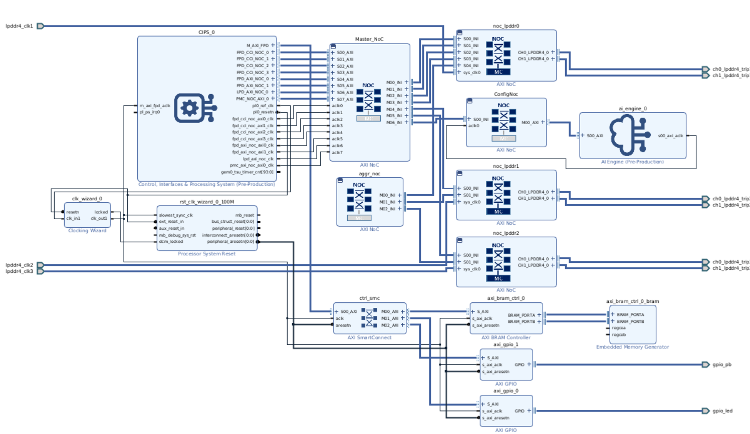
VCK190 base block design.
PL Payload:
PS Specifications:
The following default PS configuration is implemented in the embedded common platform CED for Zynq Ultrascale+, and is aligned with common specifications, there are also some board defined items such as fixed MIO, clocks, and enabling clock frequencies enabled by the speed grade of the target device.
PS Peripheral mappings in the CED
AXI BRAM Controller: Mapped to the address range for Block RAM access.
AXI GPIO (gpio_0): Mapped to EMIO interface with 256 GPIO signals.
AXI GPIO (gpio_1): Mapped to EMIO interface with 256 additional GPIO signals.
AI Engine: Mapped to a configurable address space for AI processing.
Master NoC: Mapped to system’s AXI address space for interconnectivity.
AXI NoCs: Mapped to address range facilitating access between different IP blocks.
Clocking Wizard: Mapped to the address space for clock signal management.
Timers: Mapped to EMIO interface with event generation capabilities.
DDR Memory Interfaces: Mapped to the address space connecting LPDDR4 memory.
I2C (0): Mapped to MIO pins for connecting to external devices (specific pins per design).
UART (Serial Communication): Mapped to MIO pins for serial data transfer (specific pins per design).
SPI (Serial Peripheral Interface): Mapped to MIO pins for SPI connections (specific pins per design).
Interrupts
PS-PL Interrupts
The embedded common platform CED enables one LPD interrupt.
The following table outlines the planned application mapping and utilization of the PS-PL interrupts.
Domain |
IRQ |
Enabled |
Allocation |
|---|---|---|---|
0 |
Yes |
PL Interrupts |
IPI Mappings
The embedded common platform CED enables a superset of IPI mappings to support current and future TRDs and are defined in the following table.
These do not impact the PS/PL boundary so are not controlled relative to TRD specific PL designs.
IPI / IRQ |
Enabled |
Master |
Description |
|---|---|---|---|
Yes |
|||
Yes |
|||
Yes |
IPI used by PSM (Platform Service Manager) for event signaling. |
||
IPI 0 |
Yes |
A72 |
|
IPI 1 |
Yes |
R5 0 |
Used by RPU core 0 for inter-core communication. |
IPI 2 |
Yes |
R5 1 |
Used by RPU core 1 for inter-core communication. |
IPI 3 |
Yes |
A72 |
|
IPI 4 |
Yes |
A72 |
|
IPI 5 |
Yes |
A72 |
|
IPI 6 |
Yes |
A72 |
DDR Memory Map
The following represents the map reflecting the number of RPUs and physical memory available in the platform.
Region Name |
Start Address |
Size (Bytes) |
Description |
|---|---|---|---|
C0_DDR_LOW0 |
0x0000_0000 |
2 GB |
DDR region on Controller 0, Channel 0 |
C0_DDR_LOW1 |
0x8000_0000 |
2 GB |
DDR region on Controller 0, Channel 1 |
C1_DDR_CH1 |
0x5000_0000_0000 |
4 GB |
DDR region on Controller 1, Channel 1 |
C1_DDR_CH2 |
0x6000_0000_0000 |
4 GB |
DDR region on Controller 1, Channel 2 |
C2_DDR_LOW0 |
0x0000_0000 |
2 GB |
DDR region on Controller 2, Channel 0 |
C2_DDR_LOW1 |
0x8000_0000 |
2 GB |
DDR region on Controller 2, Channel 1 |
C3_DDR_LOW0 |
0x0000_0000 |
2 GB |
DDR region on Controller 3, Channel 0 |
C3_DDR_LOW1 |
0x8000_0000 |
2 GB |
DDR region on Controller 3, Channel 1 |
C1_DDR_LOW0 |
0x0000_0000 |
2 GB |
DDR region on Controller 1, Channel 0 (LPD NOC) |
C1_DDR_LOW1 |
0x8000_0000 |
2 GB |
DDR region on Controller 1, Channel 1 (LPD NOC) |
System Level Memory Map
Start Address |
Description |
|---|---|
0x0000_0000 |
DDR C0 LOW0 |
0x8000_0000 |
DDR C0 LOW1 |
0xA400_0000 |
AXI BRAM Controller |
0xA600_0000 |
AXI GPIO 0 |
0xA601_0000 |
AXI GPIO 1 |
0x2000_0000_0000 |
AI Engine Memory Space |
0x5000_0000_0000 |
DDR C1 CH1 |
0x6000_0000_0000 |
DDR C1 CH2 |
0xFFFC_0000 |
OCM |
VRK160
Boot Firmware and Linux Disk Images
Boot Firmware Images - OSPI VRK160 - Boot Firmware + boot.pdi:
Refer to Common Specifications
Linux Disk Image - Common Disk Image With Support for This Board
Refer to Common Specifications
VRK160 OSPI Memory Map
OSPI Device Specifications:
Device: Micron 2Gbit Octal SPI Flash Memory (MT35XU02GCBA1G12-0SIT)
Capacity: 256 MB (2Gbit)
Configuration: 24-ball T-PBGA, 05/6 mm x 8 mm (5x5 array)
Interface: OSPI with PS_MODE[3:0] set to “1000”
Operating Temperature: –40°C to 85°C
Clock Frequency: Maximum 200 MHz in DDR mode
Memory Map Table:
Start Address |
Description |
Size (MB) |
Size (KB) |
Start Sector |
R or R/W |
MTD |
MultiBoot Offset |
|---|---|---|---|---|---|---|---|
0x0000_0000 |
Boot Header/Image Selector |
1 |
1024 |
0 |
R |
mtd0 |
0x0000 |
0x0010_0000 |
PLM (Platform Loader Manager) |
2 |
2048 |
16 |
R |
mtd1 |
|
0x0030_0000 |
1 |
1024 |
48 |
R |
mtd2 |
||
0x0040_0000 |
4 |
4096 |
64 |
R |
mtd3 |
||
0x0080_0000 |
Linux Kernel Image |
32 |
32768 |
128 |
R |
mtd4 |
|
0x0280_0000 |
Device Tree Blob |
1 |
1024 |
640 |
R |
mtd5 |
|
0x0290_0000 |
Root Filesystem |
128 |
131072 |
656 |
R |
mtd6 |
|
0x0A90_0000 |
User Data/Configuration |
32 |
32768 |
2704 |
R/W |
mtd7 |
|
0x0C90_0000 |
Recovery/Golden Image |
32 |
32768 |
3216 |
R |
mtd8 |
0x0C90_0000 |
0x0E90_0000 |
Bitstream Storage |
24 |
24576 |
3728 |
R/W |
mtd9 |
|
0x1010_0000 |
Reserved |
16 |
16384 |
4112 |
VRK160 DDR Memory Map
Start Addr |
Size (MB) |
Description |
Fixed/Variable |
XMPU |
|---|---|---|---|---|
0x0000_0000 |
2048 |
DDR_CH0_LEGACY - Low Memory Region |
Fixed |
XMPU0 |
0x8000_0000 |
0 |
Reserved |
||
0x0008_0000_0000 |
2048 |
DDR_CH0_MED - Extended Memory Region |
Fixed |
XMPU1 |
0x0500_0000_0000 |
4096 |
DDR_CH1 - Channel 1 Memory |
Fixed |
XMPU2 |
0x0600_0000_0000 |
4096 |
DDR_CH2 - Channel 2 Memory |
Fixed |
XMPU3 |
0x0700_0000_0000 |
4096 |
DDR_CH3 - Channel 3 Memory |
Fixed |
XMPU4 |
VRK160 Programing/flashing the OSPI (Primary Boot Device)
See
VRK160 Programing the SD Card / UFS (Secondary Boot device)
VRK160 Basic Board Interfaces
The following describes the location of the basic board interfaces.
Basic Board Setup:
Connect the external power supply to the “Power Input” connector
12 V DC power input
Connected to the Digital Power Supplies module
Connect the USB cable to the “FTDI USB” interface to the host PC
Connect the RJ45 connector to the local network
Connected through the K24 System Controller
Provides network connectivity for system management
Connect the SD Card to the “uSD 3.0” slot
MicroSD card slot for secondary boot and storage
Supports up to UHS-I speeds
VRK160 Powering the Board
To power up the board, connect the board external power supply to an outlet, plug in the external supply to the VRK160 board and turn the board on with the power switch.
Configuration Modes (MODE[3:0])
The VRK160 uses a 4-position DIP switch with pulldown resistors to
configure the boot mode. The MODE[3:0] pins are connected to the Versal
device through the System Controller. The System Controller
PS MIO pins are connected to MODE[3:0], allowing isolation
through open-drain buffers for reading the user-selected boot mode.
DIP Switch Configuration :
Boot Mode |
Mode Pins [3:0] |
DIP Switch Setting |
Interface |
Description |
|---|---|---|---|---|
JTAG |
0000 |
OFF-OFF-OFF-OFF |
JTAG Dedicated IO |
JTAG boot mode for debugging |
OSPI |
1000 |
OFF-OFF-OFF-ON |
PMC_MIO |
Default boot mode - Boot from OSPI flash |
SD1 3.0 |
1110 |
OFF-ON-ON-ON |
PMC_MIO |
Boot from SD card slot |
VRK160 System Controller Firmware Update
See the System Controller Wiki for more information https://xilinx-wiki.atlassian.net/wiki/x/AYCGhw
VRK160 UART connections - FTDI-USB
The VRK160 has four serial / UART interfaces. The four UART are mapped as follows,
System Controller (K24) |
DUT (S71/S72) |
|
|---|---|---|
ADBUS (Device 0) |
||
BDBUS (Device 1) |
SC-UART0 |
PS-UART0 |
CDBUS (Device 2) |
SC-UART1 |
|
DDBUS (Device 3) |
PS-UART1 |
Connection Details:
ADBUS (Device 0):
Direct JTAG connection to S71/S72
Used for programming and debugging
No System Controller involvement
BDBUS (Device 1):
System Controller UART0 monitors PS-UART0
Primary PS console output
Boot messages and Linux console
CDBUS (Device 2):
System Controller UART1 monitors PL-UART
Programmable Logic debug output
User application console from PL
DDBUS (Device 3):
VRK160 Ethernet Connections
Ethernet Interface Overview
The VRK160 board provides Ethernet connectivity through the K24 System Controller, which manages network interfaces for both system management and user applications.
Ethernet Connection Details
Interface |
Connector |
Controller |
Speed |
Purpose |
|---|---|---|---|---|
System Controller Ethernet |
RJ45 |
10/100/1000 Mb/s |
Board management, configuration |
|
PS Ethernet (if available) |
Through K24 |
S71/S72 PS |
10/100/1000 Mb/s |
User applications |
VRK160 Base Vivado Design for BSPs and PS specifications
This specification inherits from the common and device specific specifications but also has evaluation board specific items. See also the following:
VRK160 PL Board I/O
Interface |
Connector/Component |
Type |
Specifications |
PL Bank |
Voltage |
Purpose |
|---|---|---|---|---|---|---|
FMC+ (FMCP GEN I/Os) |
FMCP Connector |
High-Speed I/O |
FMC+ HPC Standard |
Multiple |
1.2 V-3.3 V |
Expansion cards, Custom I/O |
HD I/O |
Board Edge |
Differential I/O |
High-speed differential pairs |
HD I/O Banks |
1.2 V |
High-speed serial protocols |
XSIO (Extended Serial I/O) |
Board Edge |
Serial I/O |
Multi-gigabit transceivers |
GTY Banks |
1.2 V |
Serial protocols, PCIe |
PL UART |
115200,8,N,1 |
HP Bank |
3.3 V |
PL debug console |
||
ADC Interface |
Carlisle Connector |
Analog Input |
High-speed ADC |
Analog |
Data acquisition, DSP |
|
DAC Interface |
Carlisle Connector |
Analog Output |
High-speed DAC |
Analog |
Waveform generation |
|
RF CLK SMA |
SMA Connectors |
Clock I/O |
DC-6 GHz |
Clock-capable |
1.8 V |
RF clock input/output |
Memory CLK SMA |
SMA Connectors |
Clock I/O |
LPDDR5X clocks |
Clock-capable |
1.8 V |
Memory clock probe |
General Purpose SMA |
SMA Connectors |
Flexible I/O |
DC-6 GHz |
HP Banks |
1.8 V |
Test points, triggers |
GPIO Headers |
Pin Headers |
Digital I/O |
User-defined |
HP Banks |
1.8 V/3.3 V |
General purpose I/O |
CSPF56 |
CSPF56 Connector |
Mixed Signal |
56-pin interface |
Multiple |
1.8 V/3.3 V |
Custom expansion |
SYSMON Header |
Pin Header |
Monitor |
Analog monitoring |
Analog |
System monitoring |
|
Board EEPROM |
I2C Device |
Storage |
256 bytes min |
HP Bank |
3.3 V |
Board ID, user data |
VRK160 MMI Configuration
Memory-Mapped Interface (MMI) Overview
The VRK160 provides several MMI configuration options for system monitoring and control.
MMI Components:
SYSMON Header
System monitoring interface
Temperature and voltage monitoring
Connected to Versal System Monitor
Provides real-time telemetry data
General Purpose SMAs
SubMiniature version A connectors
Flexible signal routing
Can be configured for:
Clock inputs/outputs
Trigger signals
Test points
Custom I/O
Memory CLK SMAs
Dedicated SMA connectors for memory clocking
LPDDR5X clock connections:
2x16 interface
1x32 interface (x2)
Enables external clock injection for testing
Supports clock monitoring and measurement
MMI Configuration Options:
Software-configurable through Versal CIPS
Hardware strapping options through DIP switches
Runtime configuration through System Controller
VRK160 MMI Clocks
Clock Architecture Overview
The VRK160 implements a sophisticated clocking scheme to support various interfaces and performance requirements.
Primary Clock Sources:
SI5518 Clock Generator
Reference clock generator
Programmable output frequencies
Low-jitter performance
I2C programmable
Provides system reference clocks
SI95314 Clock Generators (x2)
Two independent clock generator ICs
Multiple output channels
Support for different clock domains
Programmable through I2C interface
RF CLK SMAs
RF clock interfaces through SMA connectors
Support for external clock injection
Clock distribution to RF sections
Enables synchronization with external equipment
VRK160 Reference PL Payload Information
See the Discovery and Evaluation
ZC702
Default Boot Flow
The default boot flow for the EDF Linux BSP for ZC702 is Common Specifications
See Common Specifications for more information.
ZC702 Boot Firmware and Linux Disk Images
Boot Firmware Images
Not applicable
Linux Disk Image - Common Disk Image With Support for This Board
edf-linux-disk-image-amd-cortexa9thf-neon-common+zynq-zc702-sdt-full.rootfs.wic.xz
Advanced Embedded Software Configurations Included
None
OpenAMP and XEN to follow in a future release
ZC702 UART Interfaces:
USB-to-UART Bridge Overview
The ZC702 board contains a Silicon Labs CP2103GM USB-to-UART bridge device (U36) which allows a connection to a host computer with a USB port. The USB cable is supplied in the ZC702 Evaluation Kit. The CP2103GM is powered by the USB 5 V provided by the host PC when the USB cable is plugged into the USB port on the ZC702 board.
Key Features:
Bridge IC: CP2103GM 1X and 4X pins (Silicon Labs)
Location: U36 on the board
Power: USB 5 V powered from host PC
Drivers: Silicon Labs provides royalty-free Virtual COM Port (VCP) drivers
USB Connector Pin Assignments (J17)
USB Connector (J17) Pin |
Net Name |
Description |
CP2103GM (U36) Pin |
Name |
|---|---|---|---|---|
1 |
VBUS |
USB UART_VBUS |
+5 V VBUS Powered |
7 |
2 |
D_N |
USB UART_D_N |
Bidirectional differential serial data (N side) |
5 |
3 |
D_P |
USB UART_D_P |
Bidirectional differential serial data (P side) |
4 |
5 |
GND |
USB_UART_GND |
Signal ground |
2 |
UART Signal Definitions
The USB Connector pin assignments and signal definitions between J17 and U36 are listed in Table 1-15.
XC7Z020 SoC to CP2103 Connections
XC7Z020 SoC (U1) Bank 500 |
CP2103GM Device (U36) |
|||
|---|---|---|---|---|
Pin Name |
Pin Number |
Function |
Direction |
Net Name |
PS_MIO14 |
D11 |
TX |
O |
USB_UART_RX |
PS_MIO15 |
E14 |
RX |
I |
USB_UART_TX |
ZC702 Ethernet connections
ZC702 base design (CED) and PS specifications
CED Overview
The ZC702 Configurable Example Design (CED) provides a base platform for Zynq-7000 development with pre-configured PS and basic PL infrastructure.
ZC702 Configurable Example Design (CED) base block design.
Base Design Components:
Processing System (PS):
Zynq-7020 (XC7Z020-CLG484)
Dual-core Arm Cortex-A9 @ 667 MHz
DDR3 interface configured
Standard peripheral set enabled
PL Infrastructure:
PS Specifications
Processor Configuration:
Dual Arm Cortex-A9 cores
32 KB L1 I-cache, 32 KB L1 D-cache per core
512 KB shared L2 cache
NEON SIMD extensions
VFPv3 floating point
Memory Interfaces:
DDR3: 1 GB @ 533 MHz (1066MT/s), 32-bit wide
QSPI: 128 Mb flash for boot
OCM: 256 KB on-chip memory
Clock Configuration:
ZC702 Processing System Peripheral Mappings in the Configurable Example Design
Peripheral |
MIO Pins |
Function |
Notes |
|---|---|---|---|
UART1 |
MIO 48-49 |
Console UART |
115200 baud |
USB0 |
MIO 28-39 |
USB 2.0 Host/Device |
ULPI interface |
GEM0 |
MIO 16-27 |
Gigabit Ethernet |
RGMII to PHY |
SD0 |
MIO 40-45 |
SD Card |
4-bit mode |
QSPI |
MIO 1-6 |
Boot Flash |
Single I/O mode |
GPIO |
MIO 0, 7, 8-15, 46-47, 50-51 |
Various |
Buttons, LEDs |
PL Payload
Default Payload - Basic Platform:
Components:
Interrupts
PS Peripheral Interrupt Mappings
IRQ ID |
Interrupt Source |
Description |
|---|---|---|
0-15 |
SGI[0:15] |
Software Generated Interrupts |
27 |
CPU Global Timer |
Arm Cortex-A9 global timer |
29 |
CPU Private Timer |
Arm Cortex-A9 private timer |
30 |
Arm Cortex-A9 private watchdog |
|
32 |
L2 Cache |
L2 cache controller interrupt |
33 |
OCM |
On-chip memory controller |
35 |
PMU0 |
Performance monitor unit CPU0 |
36 |
PMU1 |
Performance monitor unit CPU1 |
37 |
XADC |
System monitor interrupt |
38 |
DevC/PCAP |
Device configuration interrupt |
39 |
SWDT |
System watchdog timer |
40 |
TTC0_0 |
Triple timer counter 0, timer 0 |
41 |
TTC0_1 |
Triple timer counter 0, timer 1 |
42 |
TTC0_2 |
Triple timer counter 0, timer 2 |
43 |
DMAC_Abort |
DMA controller abort |
44 |
DMAC0 |
DMA channel 0 |
45 |
DMAC1 |
DMA channel 1 |
46 |
DMAC2 |
DMA channel 2 |
47 |
DMAC3 |
DMA channel 3 |
48 |
SMC |
Static memory controller |
49 |
QSPI |
Quad-SPI controller |
50 |
GPIO |
GPIO controller |
51 |
USB0 |
USB controller 0 |
52 |
GEM0 |
Gigabit Ethernet MAC 0 |
53 |
GEM0_Wake |
GEM0 wake on LAN |
54 |
SDIO0 |
SD/SDIO controller 0 |
55 |
I2C0 |
I2C controller 0 |
56 |
SPI0 |
SPI controller 0 |
57 |
UART0 |
UART controller 0 |
58 |
CAN0 |
CAN controller 0 |
59 |
FPGA0 |
|
60 |
FPGA1 |
|
61 |
FPGA2 |
|
62 |
FPGA3 |
|
63 |
FPGA4 |
|
64 |
FPGA5 |
|
65 |
FPGA6 |
|
66 |
FPGA7 |
|
67 |
TTC1_0 |
Triple timer counter 1, timer 0 |
68 |
TTC1_1 |
Triple timer counter 1, timer 1 |
69 |
TTC1_2 |
Triple timer counter 1, timer 2 |
70 |
DMAC4 |
DMA channel 4 |
71 |
DMAC5 |
DMA channel 5 |
72 |
DMAC6 |
DMA channel 6 |
73 |
DMAC7 |
DMA channel 7 |
74 |
USB1 |
USB controller 1 |
75 |
GEM1 |
Gigabit Ethernet MAC 1 |
76 |
GEM1_Wake |
GEM1 wake on LAN |
77 |
SDIO1 |
SD/SDIO controller 1 |
78 |
I2C1 |
I2C controller 1 |
79 |
SPI1 |
SPI controller 1 |
80 |
UART1 |
UART controller 1 |
81 |
CAN1 |
CAN controller 1 |
82 |
FPGA8 |
|
83 |
FPGA9 |
|
84 |
FPGA10 |
|
85 |
FPGA11 |
|
86 |
FPGA12 |
|
87 |
FPGA13 |
|
88 |
FPGA14 |
|
89 |
FPGA15 |
|
90 |
Parity |
RAM parity error |
PS-PL Interrupts
Interrupt Signal |
IRQ ID |
Direction |
Description |
|---|---|---|---|
IRQ_F2P[0] |
59 |
Fabric to PS interrupt 0 |
|
IRQ_F2P[1] |
60 |
Fabric to PS interrupt 1 |
|
IRQ_F2P[2] |
61 |
Fabric to PS interrupt 2 |
|
IRQ_F2P[3] |
62 |
Fabric to PS interrupt 3 |
|
IRQ_F2P[4] |
63 |
Fabric to PS interrupt 4 |
|
IRQ_F2P[5] |
64 |
Fabric to PS interrupt 5 |
|
IRQ_F2P[6] |
65 |
Fabric to PS interrupt 6 |
|
IRQ_F2P[7] |
66 |
Fabric to PS interrupt 7 |
|
IRQ_F2P[8] |
82 |
Fabric to PS interrupt 8 |
|
IRQ_F2P[9] |
83 |
Fabric to PS interrupt 9 |
|
IRQ_F2P[10] |
84 |
Fabric to PS interrupt 10 |
|
IRQ_F2P[11] |
85 |
Fabric to PS interrupt 11 |
|
IRQ_F2P[12] |
86 |
Fabric to PS interrupt 12 |
|
IRQ_F2P[13] |
87 |
Fabric to PS interrupt 13 |
|
IRQ_F2P[14] |
88 |
Fabric to PS interrupt 14 |
|
IRQ_F2P[15] |
89 |
Fabric to PS interrupt 15 |
IPI Mappings
Zynq-7000 uses Software Generated Interrupts (SGI) for Inter-Processor Interrupts:
SGI ID |
Source |
Target |
Description |
|---|---|---|---|
0 |
CPU0/CPU1 |
CPU0/CPU1 |
User defined IPI |
ZC702 DDR Memory Map
The ZC702 board features DDR3 memory connected to the Zynq-7000 Processing System. Here is the memory map:
DDR3 Memory Specifications
Memory Type: DDR3 SDRAM
Capacity: 1 GB (standard configuration)
Data Width: 32-bit
Speed: 533 MHz (1066MT/s)
DDR Memory Map Table
Start Address |
End Address |
Size |
Description |
Access Type |
Notes |
|---|---|---|---|---|---|
0x0000_0000 |
0x3FFF_FFFF |
1 GB |
DDR3 SDRAM |
R/W |
Main system memory |
ZC702 System Level Memory Map
Start Address |
Description |
|---|---|
0x00000000 |
DDR3 SDRAM (1 GB) |
0x40000000 |
|
0x41200000 |
AXI GPIO (LEDs) |
0x41C00000 |
AXI BRAM Controller |
0x80000000 |
|
0xE0000000 |
IOP Peripherals - UART0 |
0xE0001000 |
IOP Peripherals - UART1 |
0xE0002000 |
IOP Peripherals - USB0 |
0xE0003000 |
IOP Peripherals - USB1 |
0xE0004000 |
IOP Peripherals - I2C0 |
0xE0005000 |
IOP Peripherals - I2C1 |
0xE0006000 |
IOP Peripherals - SPI0 |
0xE0007000 |
IOP Peripherals - SPI1 |
0xE0008000 |
IOP Peripherals - CAN0 |
0xE0009000 |
IOP Peripherals - CAN1 |
0xE000A000 |
IOP Peripherals - GPIO |
0xE000B000 |
IOP Peripherals - GEM0 (Ethernet) |
0xE000C000 |
IOP Peripherals - GEM1 |
0xE000D000 |
IOP Peripherals - QSPI Controller |
0xE000E000 |
IOP Peripherals - SMC |
0xE0100000 |
IOP Peripherals - SD0 |
0xE0101000 |
IOP Peripherals - SD1 |
0xE0200000 |
Triple Timer Counter 0 |
0xE0201000 |
Triple Timer Counter 1 |
0xE1000000 |
SMC - SRAM/NOR Memory |
0xF8000000 |
SLCR (System Level Control Registers) |
0xF8001000 |
PS Clock Control |
0xF8002000 |
PS Reset Control |
0xF8003000 |
DDR Controller Registers |
0xF8004000 |
Device Configuration (DEVC) |
0xF8005000 |
AXI FIFO Interface 0 (AFI0) |
0xF8006000 |
AXI FIFO Interface 1 (AFI1) |
0xF8007000 |
AXI FIFO Interface 2 (AFI2) |
0xF8008000 |
AXI FIFO Interface 3 (AFI3) |
0xF8009000 |
OCM Configuration |
0xF800C000 |
eFUSE Controller |
0xF8800000 |
L2 Cache Controller (PL310) |
0xF8890000 |
SCU (Snoop Control Unit) |
0xF8891000 |
SCU Global Timer |
0xF8F00000 |
Private Timer and Watchdog |
0xF8F01000 |
Interrupt Controller Distributor |
0xF8F02000 |
Interrupt Controller CPU Interface |
0xFC000000 |
QSPI Linear Mode (32 MB) |
0xFFFC0000 |
OCM (On-Chip Memory) 256 KB |
Additional Memory Regions for PL Access
Start Address |
Description |
|---|---|
0x43C00000 |
Reserved for Custom AXI IP |
0x43C10000 |
Reserved for Custom AXI IP |
0x43C20000 |
Reserved for Custom AXI IP |
0x43C30000 |
Reserved for Custom AXI IP |
0x83C00000 |
Reserved for AXI IP through GP1 |
0x83C10000 |
Reserved for AXI IP through GP1 |
ZC706
Default Boot Flow
For the default boot flow of the EDF Linux Board Support Package (BSP) for ZC706, refer to Common Specifications.
ZC706 Boot Firmware and Linux Disk Images
Boot Firmware Images
Not applicable
Linux Disk Image - Common Disk Image With Support for This Board
edf-linux-disk-image-amd-cortexa9thf-neon-common+zynq-zc706-sdt-full.rootfs.wic.xz
Advanced Embedded Software Configurations Included
None
OpenAMP and Xen to follow in a future release
ZC706 Universal Asynchronous Receiver-Transmitter Interfaces
This section describes the USB-to-UART bridge implementation and the corresponding connector and SoC signal mappings for ZC706.
USB-to-UART Bridge Overview
The ZC706 board contains a Silicon Labs CP2103GM USB-to-UART bridge device (U23). It connects the board to a host computer through a USB port. The ZC706 Evaluation Kit includes the USB cable. The host PC supplies USB 5 V to the CP2103GM after you connect the cable to the USB port on the ZC706 board.
Key Features
Bridge IC: CP2103GM (Silicon Labs)
Location: U23 on the board
Power: USB 5 V powered from host PC
Drivers: Silicon Labs provides royalty-free Virtual COM Port (VCP) drivers
USB Connector Pin Assignments (J2)
The following table lists the USB connector (J2) signals and their mappings to CP2103GM (U23).
USB Connector (J2) Pin |
Net Name |
Description |
CP2103GM (U23) Pin |
Name |
|---|---|---|---|---|
1 |
VBUS |
USB serial VBUS +5 V VBUS powered |
7 |
VBUS |
2 |
D_N |
USB UART_D_N - Differential data (N) |
5 |
D- |
3 |
D_P |
USB UART_D_P - Differential data (P) |
4 |
D+ |
5 |
GND |
USB_UART_GND - Signal ground |
2 |
Universal Asynchronous Receiver-Transmitter Signal Definitions
The following table lists the UART signal mappings between the XC7Z045 SoC PS-MIO pins and the CP2103 bridge device.
XC7Z045 System-on-Chip to CP2103 Connections
Pin Name |
Pin Number |
Function |
Direction |
Net Name |
|---|---|---|---|---|
PS_MIO48 |
K17 |
TX |
O |
USB_UART_RX |
PS_MIO49 |
K18 |
RX |
I |
USB_UART_TX |
ZC706 Ethernet Connections
PHY Chip: Marvell Alaska 88E1116R (U67)
Speeds: 10 / 100 / 1000 Mb/s
Interface: RGMII mode
Connector: RJ-45 (P4) with integrated magnetics
ZC706 Base Design and Processing System Specifications
Configurable Example Design Overview
The ZC706 Configurable Example Design provides a base platform for Zynq-7000 XC7Z045 development with pre-configured Processing System and basic Programmable Logic infrastructure.
ZC706 Configurable Example Design (CED) block diagram
Base Design Components
Processing System (PS):
Zynq-7045 (XC7Z045-FFG900)
Dual-core Arm Cortex-A9 @ up to 800 MHz
DDR3 interface configured
Standard peripheral set enabled
PL Infrastructure:
AXI Interconnect (AXI SmartConnect)
AXI Block Memory Controller
AXI GPIO for LEDs
Processor System Reset module
Clock infrastructure (100 MHz default)
Processing System Specifications
Processor Configuration:
Dual Arm Cortex-A9 cores
32 KB L1 I-cache, 32 KB L1 D-cache per core
512 KB shared L2 cache
NEON SIMD extensions
VFPv3 floating point
Memory Interfaces:
DDR3: 1 GB (SODIMM) @ 533 MHz (1066 MT/s), 64-bit wide
QSPI: 128 Mb boot flash
OCM: 256 KB on-chip memory
Clock Configuration:
ZC706 Processing System Peripheral Mappings in the Configurable Example Design
Peripheral |
MIO Pins |
Function |
Notes |
|---|---|---|---|
UART1 |
MIO 48-49 |
Console UART |
115200 baud |
USB0 |
MIO 28-39 |
USB 2.0 Host/Device |
|
GEM0 |
MIO 16-27 |
Gigabit Ethernet |
|
SD0 |
MIO 40-45 |
SD Card |
4-bit mode |
QSPI |
MIO 1-6 |
Boot Flash |
Single I/O |
GPIO |
Multiple |
Buttons / LEDs |
N/A |
Programmable Logic Payload
The default payload is a basic platform with the following components:
AXI Interconnect
AXI Block Memory Controller
Block Memory Generator
AXI GPIO (LEDs)
Processor System Reset
ZC706 DDR Memory Map
ZC706 DDR3 Memory Specifications
Memory Type: DDR3 SDRAM
Capacity: 1 GB
Data Width: 64-bit
Speed: 533 MHz (1066 MT/s)
ZC706 DDR Memory Map Table
Start Address |
End Address |
Size |
Description |
Access |
Notes |
|---|---|---|---|---|---|
0x0000_0000 |
0x3FFF_FFFF |
1 GB |
DDR3 SDRAM |
R/W |
Main system memory |
ZC706 System Level Memory Map
The address map matches the ZC702 and preserves software compatibility.
Start Address |
Description |
|---|---|
0x00000000 |
DDR |
0xE0000000 |
PS peripherals |
0xF8000000 |
SLCR |
0xFC000000 |
QSPI linear |
0xFFFC0000 |
OCM |
ZC706 Additional Memory Regions for Programmable Logic Access
Start Address |
Description |
|---|---|
0x43C00000 |
Reserved for Custom AXI IP |
0x83C00000 |
Reserved for AXI IP through GP1 |
VPK120
Boot Firmware and Linux Disk Images
Linux Disk Image - Common Disk Image With Support for This Board
Refer to Common Specifications
VPK120 System Controller Firmware Update
See the System Controller Wiki for more information https://xilinx-wiki.atlassian.net/wiki/x/AYCGhw
VPK120 DDR Memory Map
Start Address |
End Address |
Size |
Description |
Interface |
Access Type |
|---|---|---|---|---|---|
0x0000_0000_0000 |
0x7FFF_FFFF |
2 GB |
C0_DDR_LOW0 |
NoC_lpddr0/S00_INI |
R/W |
0x0008_0000_0000 |
0x0008_7FFF_FFFF |
2 GB |
C0_DDR_LOW1 |
NoC_lpddr0/S00_INI |
R/W |
0x0500_0000_0000 |
0x0500_FFFF_FFFF |
4 GB |
C0_DDR_CH1 |
NoC_lpddr1/S00_INI |
R/W |
0x0600_0000_0000 |
0x0600_FFFF_FFFF |
4 GB |
C0_DDR_CH2 |
NoC_lpddr2/S00_INI |
R/W |
0x0500_0000_0000 |
0x0500_FFFF_FFFF |
4 GB |
C1_DDR_CH1 |
NoC_lpddr1/S00_INI |
R/W |
0x0600_0000_0000 |
0x0600_FFFF_FFFF |
4 GB |
C1_DDR_CH2 |
NoC_lpddr2/S00_INI |
R/W |
0x0500_0000_0000 |
0x0500_FFFF_FFFF |
4 GB |
C2_DDR_CH1 |
NoC_lpddr0/S02_INI |
R/W |
0x0600_0000_0000 |
0x0600_FFFF_FFFF |
4 GB |
C2_DDR_CH2 |
NoC_lpddr0/S02_INI |
R/W |
0x0500_0000_0000 |
0x0500_FFFF_FFFF |
4 GB |
C3_DDR_CH1 |
NoC_lpddr0/S03_INI |
R/W |
0x0600_0000_0000 |
0x0600_FFFF_FFFF |
4 GB |
C3_DDR_CH2 |
NoC_lpddr0/S03_INI |
R/W |
DDR Configuration Summary:
Total DDR: Multiple LPDDR channels
Channel Configuration: 4 controllers (C0-C3)
Memory Type: LPDDR4/LPDDR5
Access: Through NoC (Network on Chip)
VPK120 System Level Memory Map
Start Address |
Description |
Size |
Type |
|---|---|---|---|
0x0000_0000_0000 |
DDR Low Memory Region 0 |
2 GB |
DDR |
0x0008_0000_0000 |
DDR Low Memory Region 1 |
2 GB |
DDR |
0x0500_0000_0000 |
DDR Channel 1 (All Controllers) |
4 GB |
DDR |
0x0600_0000_0000 |
DDR Channel 2 (All Controllers) |
4 GB |
DDR |
0xA400_0000 |
AXI BRAM Controller |
8 KB |
|
0xA401_0000 |
AXI GPIO 0 (LEDs) |
64 KB |
PL Peripheral |
0xA402_0000 |
AXI GPIO 1 (Push Buttons) |
64 KB |
PL Peripheral |
0xA403_0000 |
AXI GPIO 2 (DIP Switches) |
64 KB |
PL Peripheral |
0xF000_0000 |
CIPS Configuration Space |
PS Registers |
|
0xF100_0000 |
FPD Peripherals |
PS Peripherals |
|
0xF900_0000 |
LPD Peripherals |
PS Peripherals |
|
0xFE00_0000 |
PMC Peripherals |
||
0xFF00_0000 |
CPM/PCIe |
CPM |
PL Peripheral Details:
Base Address |
Peripheral |
Description |
Size |
|---|---|---|---|
0xA400_0000 |
Block RAM storage |
8 KB |
|
0xA401_0000 |
GPIO_0 |
LED control (gpio_led) |
64 KB |
0xA402_0000 |
GPIO_1 |
Push buttons (gpio_pb) |
64 KB |
0xA403_0000 |
GPIO_2 |
DIP switches (gpio_dp) |
64 KB |
VPK120 QSPI Memory Map
Based on typical Versal Prime configurations:
Start Address |
Description |
Size (MB) |
Start Sector |
R or R/W |
MTD |
MultiBoot Offset |
|---|---|---|---|---|---|---|
0x0000_0000 |
Boot Header |
1 |
0 |
R |
mtd0 |
0x0000 |
0x0010_0000 |
PLM Firmware |
2 |
16 |
R |
mtd1 |
|
0x0030_0000 |
2 |
48 |
R |
mtd2 |
||
0x0050_0000 |
Device Image (PDI) |
32 |
80 |
R |
mtd3 |
|
0x0250_0000 |
APU Application |
64 |
592 |
R |
mtd4 |
|
0x0650_0000 |
Linux Kernel |
32 |
1616 |
R |
mtd5 |
|
0x0850_0000 |
Device Tree |
1 |
2128 |
R |
mtd6 |
|
0x0860_0000 |
RootFS |
128 |
2144 |
R |
mtd7 |
|
0x1060_0000 |
User Data |
64 |
4192 |
R/W |
mtd8 |
|
0x1460_0000 |
Recovery Image |
32 |
5216 |
R |
mtd9 |
0x1460_0000 |
QSPI Configuration:
Interface: PMC QSPI controller
Mode: Quad I/O (x4)
Boot Device: Primary boot source
Typical Size: 512 MB or 1 GB
Sector Size: 64 KB
Programing the SD Card / UFS (Secondary Boot device)
VPK120 Basic Board Interfaces
Key Interfaces (From Block Diagram):
PCIe Interface: PCIe EP GENx x16 connector
GTY/GTM Transceivers: Multiple high-speed serial interfaces
Memory:
LPDDR4/5 (2x channels shown)
1588 CLK for precision timing
Storage:
SD 3.0 card interface
OSPI/QSPI flash
USB: USB 2.0 ULPI interfaceNetworking:
Debug: JTAG interface
Expansion:
FMC+ connector
GPIO headers
System Management:
EMIO connections
Mictor debug connector
SMA connectors for clocking
VPK120 Powering the Board
Power Configuration:
VPK120 Default DIP Switch Settings - Boot
Boot Mode Configuration:
Based on typical Versal boot modes:
Boot Mode |
MODE[3:0] |
DIP Switch |
Description |
|---|---|---|---|
0000 |
SW1: OFF-OFF-OFF-OFF |
JTAG boot for debugging |
|
QSPI32 |
0010 |
SW1: OFF-OFF-ON-OFF |
Boot from QSPI x4 |
0001 |
SW1: OFF-OFF-OFF-ON |
Boot from OSPI x8 |
|
SD1_LS |
1110 |
SW1: ON-ON-ON-OFF |
Boot from SD card |
USB |
0111 |
SW1: OFF-ON-ON-ON |
USB boot mode |
Note: Actual DIP switch location and numbering should be verified with board silkscreen.
VPK120 UART Connections - FTDI-USB
UART Configuration:
Based on the block diagram showing PS/PMC connections:
UART Channel |
Source |
Destination |
Purpose |
Default Settings |
|---|---|---|---|---|
UART0 |
PS MIO |
FTDI CH A |
Linux/APU Console |
115200,8,N,1 |
UART1 |
PMC MIO |
FTDI CH B |
PMC/PLM Console |
115200,8,N,1 |
UART2 |
EMIO |
FTDI CH C |
115200,8,N,1 |
|
UART3 |
FTDI CH D |
Spare/User defined |
115200,8,N,1 |
VPK120 Base Vivado Design for BSPs and PS specifications
This specification inherits from the common and device specific specifications, but also has evaluation board specific items. See also the following:
VPK120 PL Board I/O
PL I/O Interfaces (From Block Diagram and CED):
Interface |
Type |
Location |
Description |
|---|---|---|---|
FMC+ Connector |
High-speed expansion |
PL banks |
FMC+ HPC standard interface |
GPIO Headers |
Digital I/O |
PL banks |
General purpose I/O |
EMIO Signals |
PS-PL interface |
XPIO block |
|
Mictor Connector |
Debug interface |
PL banks |
High-speed debug connector |
SMA Connectors |
RF/Clock I/O |
PL banks |
Sub-miniature coaxial connectors |
GTY/GTM Transceivers |
High-speed serial |
Dedicated banks |
Multi-gigabit transceivers |
PL Peripherals in CED:
Controller |
Base Address |
Description |
Direction |
|---|---|---|---|
axi_gpio_0 |
0xA401_0000 |
GPIO for LEDs (gpio_led) |
Output |
axi_gpio_1 |
0xA402_0000 |
GPIO for Push Buttons (gpio_pb) |
Input |
axi_gpio_2 |
0xA403_0000 |
GPIO for DIP Switches (gpio_dp) |
Input |
axi_bram_ctrl_0 |
0xA400_0000 |
BRAM Controller |
Bidirectional |
VPK120 MMI Configuration
Memory-Mapped Interface Components:
NoC (Network on Chip) Configuration:
Multiple NoC instances for DDR access
noc_lpddr0: Primary LPDDR interface
noc_lpddr1: Secondary LPDDR interface
noc_lpddr2: Additional LPDDR interface
aggr_noc: Aggregates NoC traffic
AXI Interfaces:
- M_AXI_FPD: Full Power Domain AXI master
- FPD_CCI_NOC_0-3: Cache Coherent Interconnect
- FPD_AXI_NOC_0-1: AXI NoC interfaces
- LPD_AXI_NOC_0: Low Power Domain AXI
- PMC_NOC_AXI_0: Platform Management Controller AXI
Memory Access Configuration:
VPK120 MMI Clocks
Clock Sources (From Block Diagram):
Primary Reference Clocks:
1588 CLK: IEEE 1588 precision timing clock
USB CLK: USB reference clock
PCIe Content: PCIe reference clock
Transceiver Reference Clocks:
PL Clock Distribution:
From CIPS:
Clock Frequencies (typical):
SMA Clock Connections:
Input/Output capable
Support for external reference clocks
Clock measurement and monitoring
VPK120 Reference PL Payload Information
See the Discovery and Evaluation
V80
Note
The Alveo V80 follows a different build and boot flow from the other Versal Gen 1 evaluation boards. The Alveo Management Resource (AMR) documentation covers V80 build steps, boot firmware, and eMMC programming. This section documents only the V80-specific hardware that the AMR flows build on: DDR memory map, configuration device options, board interfaces, and the CED block design. A follow-up PR will add the build- and boot-step cross-references to the AMR documentation once those URLs are stable.
Boot Firmware and Linux Disk Images
The Alveo Management Resource (AMR) flow delivers the Alveo V80 boot
firmware (boot.pdi) and Linux disk image. The Alveo Management
Resource documentation describes the V80-specific images and the
flashing procedure. The common-disk-image and OSPI
boot-firmware descriptions in Common Specifications do not apply to V80.
DDR Memory Map
Region Name |
Start Address |
Size |
Description |
Interface |
|---|---|---|---|---|
C3_DDR_LOW1 |
0x0000_0000 |
2 GB |
DDR4 Controller 3, Low Region 1 |
S00_AXI |
C3_DDR_LOW0 |
0x0 |
2 GB |
DDR4 Controller 3, Low Region 0 |
S00_AXI |
C3_DDR_CH1 |
0x0500_0000_0000 |
16 GB |
DDR4 Controller 3, Channel 1 |
S00_INI |
C2_DDR_LOW1 |
0x0000_0000 |
2 GB |
DDR4 Controller 2, Low Region 1 |
S01_AXI |
C2_DDR_LOW0 |
0x0 |
2 GB |
DDR4 Controller 2, Low Region 0 |
S01_AXI |
C2_DDR_CH1 |
0x0500_0000_0000 |
16 GB |
DDR4 Controller 2, Channel 1 |
S01_INI |
C0_DDR_LOW1 |
0x0000_0000 |
2 GB |
DDR4 Controller 0, Low Region 1 |
S02_AXI |
C0_DDR_LOW0 |
0x0 |
2 GB |
DDR4 Controller 0, Low Region 0 |
S02_AXI |
C0_DDR_CH1 |
0x0500_0000_0000 |
16 GB |
DDR4 Controller 0, Channel 1 |
S02_INI |
C1_DDR_LOW1 |
0x0000_0000 |
2 GB |
DDR4 Controller 1, Low Region 1 |
S03_AXI |
C1_DDR_LOW0 |
0x0 |
2 GB |
DDR4 Controller 1, Low Region 0 |
S03_AXI |
C1_DDR_CH1 |
0x0500_0000_0000 |
16 GB |
DDR4 Controller 1, Channel 1 |
S03_INI |
Total DDR4 Memory: 5x16 DDR4 DIMM slots (64b+8b ECC)
Programming/Flashing the ACAP Configuration Flash
Primary Configuration Device:
Programming the eMMC (Secondary Storage)
eMMC Specifications:
Capacity: 64 GB
Interface: Bank 500
Usage: Secondary boot device, user data storage
The Alveo Management Resource (AMR) flow owns eMMC programming on V80, not the procedures in this docset. See the Alveo Management Resource documentation for the supported programming path (post-boot from Linux, or out-of-band through JTAG).
Basic Board Interfaces
Interface |
Type |
Specification |
|---|---|---|
PCIe |
Gen5 x8x8 |
Expansion PCIe connector |
QSFP56 |
4 ports |
PAM4 56G x4 per port |
GTM Transceivers |
GTM 209, 210, 112, 111 |
High-speed serial |
Memory |
DDR4 |
5x DIMM slots with ECC |
Configuration |
SPI Flash |
2 GB ACAP config |
Storage |
eMMC |
64 GB |
Debug |
USB3 |
JTAG/UART through PMBus/SMBus |
Monitoring |
IPMI |
Through EEPROM |
Sensors |
I2C |
Card sensors, Log Flash |
Powering the Board
Power Requirements:
Main Power: 12 V through PCIe edge connector
Auxiliary Power:
12V_AUX_A (2x4 connector)
12V_AUX_B (2x4 connector)
Power Rails: 3.3 V aux/3.3 V/12 V
Power Management:
CPMS (GTY 105-102)
XLT SMBus interface
IPMI EEPROM for monitoring
UART Connections
Debug Interface:
PL Board I/O
High-Speed I/O:
Interface |
Banks |
Type |
Count |
|---|---|---|---|
QSFP56 Port 1 |
GTM 209 |
PAM4 56G x4 |
1 |
QSFP56 Port 2 |
GTM 210 |
PAM4 56G x4 |
1 |
QSFP56 Port 3 |
GTM 112 |
PAM4 56G x4 |
1 |
QSFP56 Port 4 |
GTM 111 |
PAM4 56G x4 |
1 |
Memory I/O:
Interface |
Banks |
Type |
|---|---|---|
DDR4 DIMM |
700-702, 703-705 |
64b+8b ECC |
MCIO |
GTY 200, 213, 214, 218 |
x4, x8, x4 configurations |
Expansion:
PCIe Gen5 edge connector
Expansion sideband through QSFP
NoC Configuration
NoC Architecture:
NoC Connections:
M00_INI to M03_INI: Master interfaces
S00_AXI to S05_AXI: Slave interfaces
CHO_DDR4_0: DDR4 channel interface
Alveo V80 CED Information
A picture of the block design generated is shown in the following figure:
PL Payload:
Default payload: High-Performance Networking and Compute Platform
AXI_NOC_0
Provides high-bandwidth interconnect between CIPS and memory subsystem
Supports multiple FPD CCI interfaces for cache-coherent data access
AXI_NOC_1
Dedicated DDR4 memory NoC
Interfaces with 4 independent DDR4 controllers for parallel memory access
GTM transceiver Logic
GTM 209, 210, 112, 111: Support for 4x QSFP56 ports (PAM4 56G x4)
Enables 200G/400G Ethernet connectivity
PCIe Gen5 Endpoint
Gen5 x8x8 configuration
High-speed host interface for data movement
Memory Controller Interfaces
4x DDR4 controllers (C0-C3)
Support for 5x16 DDR4 DIMM with ECC
Distributed memory mapping for optimal bandwidth
Additional Payloads:
Network Acceleration: SmartNIC functions, packet processing
Storage Acceleration: NVMe-oF, compression/decompression
Computational Storage: In-storage compute functions
Custom Acceleration: User-defined accelerators through remaining PL
PS Specifications:
The Alveo V80 uses a Versal ACAP architecture with the following configuration:
CIPS (Control, Interfaces & Processing System) Configuration:
VPK120 PS Peripheral Mappings in the CED
High-Speed Interfaces:
GTM 209-210: QSFP56 Ports 1-2 (PAM4 56G x4)
GTM 111-112: QSFP56 Ports 3-4 (PAM4 56G x4)
GTY 200, 213, 214, 218: MCIO expansion interfaces
Memory Interfaces:
DDR4 Controller 0: Bank 700-702 (64b+8b ECC)
DDR4 Controller 1: Bank 703-705 (64b+8b ECC)
DDR4 Controller 2: Through NoC S01 interface
DDR4 Controller 3: Through NoC S00 interface
Configuration & Management:
SPI x8: Bank 500 - ACAP configuration flash (2 GB)
eMMC: Bank 500 - 64 GB storage
SMBus: XLT interface for power management
PMBus: Connected through USB3 for debug
System Interfaces:
PCIe: Gen5 x8x8 edge connector
USB3: JTAG/UART0 debug interfaceIPMI: EEPROM-based platform management
NoC Connections:
FPD_CCI_NOC_0-4: Cache coherent interfaces @ sys_clk0
PMC_NOC_AXI_0: Platform management @ pmc_axi_noc_clkLPD_AXI_NOC: Low power domain @ lpd_axi_noc_clk
Clock Distribution:
VMK180
Boot Firmware and Linux Disk Images
Linux Disk Image - Common Disk Image With Support for This Board
Refer to Common Specifications
System Controller Firmware Update
See the System Controller Wiki for more information https://xilinx-wiki.atlassian.net/wiki/x/AYCGhw
OSPI Memory Map Table
Start Address |
Description |
Size (MB) |
Start Sector |
R or R/W |
MTD |
MultiBoot Offset |
|---|---|---|---|---|---|---|
0x0000_0000 |
Boot Header/Image Selector |
2 |
0 |
R |
mtd0 |
0x0000 |
0x0020_0000 |
PLM (Platform Loader Manager) |
4 |
32 |
R |
mtd1 |
|
0x0060_0000 |
4 |
96 |
R |
mtd2 |
||
0x00A0_0000 |
NPI Configuration |
4 |
160 |
R |
mtd3 |
|
0x00E0_0000 |
CFI Configuration |
4 |
224 |
R |
mtd4 |
|
0x0120_0000 |
Primary PDI (Device Image) |
128 |
288 |
R |
mtd5 |
|
0x0920_0000 |
AI Engine Configuration |
32 |
2336 |
R |
mtd6 |
|
0x0B20_0000 |
16 |
2848 |
R |
mtd7 |
||
0x0C20_0000 |
Linux Kernel |
32 |
3104 |
R |
mtd8 |
|
0x0E20_0000 |
Device Tree Blob |
2 |
3616 |
R |
mtd9 |
|
0x0E40_0000 |
Root Filesystem |
128 |
3648 |
R |
mtd10 |
|
0x1640_0000 |
User Application Space |
64 |
5696 |
R/W |
mtd11 |
|
0x1A40_0000 |
Recovery/Golden Image |
128 |
6720 |
R |
mtd12 |
0x1A40_0000 |
0x2240_0000 |
MultiBoot Secondary |
128 |
8768 |
R |
mtd13 |
0x2240_0000 |
0x2A40_0000 |
Reserved/Future Use |
88 |
10816 |
Start Address |
Description |
Size (MB) |
Access |
Purpose |
|---|---|---|---|---|
0x0000_0000 |
Boot Header |
4 |
R |
Initial boot |
0x0040_0000 |
PLM Firmware |
8 |
R |
Platform management |
0x00C0_0000 |
8 |
R |
Configuration |
|
0x0140_0000 |
Primary PDI |
256 |
R |
PL configuration |
0x1140_0000 |
Secondary PDI |
256 |
R |
Alternate config |
0x2140_0000 |
APU App/OS |
256 |
R |
Linux/RTOS |
0x3140_0000 |
User Data |
512 |
R/W |
Application data |
0x5140_0000 |
Recovery Image |
256 |
R |
Golden image |
0x7140_0000 |
MultiBoot Backup |
256 |
R |
Failover image |
System Level Memory Map
Start Address |
End Address |
Size |
Description |
Type |
|---|---|---|---|---|
DDR Memory Regions |
||||
0x0000_0000 |
0x7FFF_FFFF |
2 GB |
C0_DDR_LOW0 - DDR4 UDIMM |
DDR4 |
0x0008_0000_0000 |
0x0009_7FFF_FFFF |
6 GB |
C0_DDR_LOW1 - DDR4 UDIMM |
DDR4 |
0x0500_0000_0000 |
0x0503_FFFF_FFFF |
4 GB |
C0_DDR_CH1 - DDR4 Channel 1 |
DDR4 |
0x0600_0000_0000 |
0x0603_FFFF_FFFF |
4 GB |
C0_DDR_CH2 - DDR4 Channel 2 |
DDR4 |
0x0000_0000 |
0x7FFF_FFFF |
2 GB |
C1_DDR_LOW0 - LPDDR4 Controller 1 |
LPDDR4 |
0x0008_0000_0000 |
0x0009_7FFF_FFFF |
6 GB |
C1_DDR_LOW1 - LPDDR4 Controller 1 |
LPDDR4 |
0x0500_0000_0000 |
0x0503_FFFF_FFFF |
4 GB |
C1_DDR_CH1 - LPDDR4 Channel 1 |
LPDDR4 |
0x0600_0000_0000 |
0x0603_FFFF_FFFF |
4 GB |
C1_DDR_CH2 - LPDDR4 Channel 2 |
LPDDR4 |
0x0000_0000 |
0x7FFF_FFFF |
2 GB |
C2_DDR_LOW0 - LPDDR4 Controller 2 |
LPDDR4 |
0x0008_0000_0000 |
0x0009_7FFF_FFFF |
6 GB |
C2_DDR_LOW1 - LPDDR4 Controller 2 |
LPDDR4 |
PL Memory Mapped Peripherals |
||||
0xA401_0000 |
0xA401_1FFF |
8 KB |
AXI BRAM Controller |
|
0xA601_0000 |
0xA601_FFFF |
64 KB |
AXI GPIO 0 (LEDs) |
PL Peripheral |
0xA602_0000 |
0xA602_FFFF |
64 KB |
AXI GPIO 1 (Push Buttons) |
PL Peripheral |
0xA603_0000 |
0xA603_FFFF |
64 KB |
AXI GPIO 2 (DIP Switches) |
PL Peripheral |
NoC Address Space |
||||
0x0200_0000_0000 |
0x021F_FFFF_FFFF |
128 GB |
NoC DDR Access Window |
|
CPM/PCIe Space |
||||
0x0400_0000_0000 |
0x047F_FFFF_FFFF |
512 GB |
PCIe Address Space |
PCIe |
PS/PMC Peripheral Space |
||||
0xF100_0000 |
0xF10F_FFFF |
1 MB |
FPD Peripherals |
|
0xF110_0000 |
0xF11F_FFFF |
1 MB |
LPD Peripherals |
|
0xF120_0000 |
0xF12F_FFFF |
1 MB |
PMC Peripherals |
|
0xF130_0000 |
0xF1FF_FFFF |
13 MB |
Reserved |
|
CIPS Configuration Space |
||||
0xF200_0000 |
0xF2FF_FFFF |
16 MB |
CIPS Control Registers |
|
RPU Memory |
||||
0xFFE0_0000 |
0xFFE3_FFFF |
256 KB |
||
OCM (On-Chip Memory) |
||||
0xFFFC_0000 |
0xFFFF_FFFF |
256 KB |
OCM |
OCM |
Boot Device Memory Windows |
||||
0xC000_0000 |
0xDFFF_FFFF |
512 MB |
QSPI Linear Mode (if enabled) |
QSPI |
System Management |
||||
0xF111_0000 |
0xF111_FFFF |
64 KB |
System Controller Interface |
|
0xF112_0000 |
0xF112_FFFF |
64 KB |
Power Management |
|
0xF113_0000 |
0xF113_FFFF |
64 KB |
Clock Control |
|
0xF114_0000 |
0xF114_FFFF |
64 KB |
Reset Control |
Programing the SD Card / UFS (Secondary Boot device)
VMK180 Basic Board Interfaces
Primary Interfaces:
Interface |
Type |
Details |
|---|---|---|
PCIe |
Gen4 x8 |
Edge connector, 8 lanes (GTY103/104) |
Ethernet |
Dual GEM |
10/100/1000, stacked RJ-45 |
USB |
USB 2.0 |
PS MIO[13:25] |
USB |
USB 3.1 Type-C |
HSDP (GTY105) |
HDMI |
TX/RX |
3 lanes TX, 1 RX (GTY106) |
SD Card |
Micro SD |
PS MIO[26:36, 50:51] |
FMC+ |
2x HSCP |
Full LA[00:33] bus |
QSFP28 |
1x cage |
4 lanes (GTY200) |
SFP28 |
2x cages |
2 lanes (GTY105) |
Memory Interfaces:
DDR4: 8 GB 72-bit UDIMM (Banks 700-702)LPDDR4: 2x 4 GB interfaces (Banks 703-705, 709-711)Boot Flash: X-EBM-01 dual QSPI module
Debug/Development:
VMK180 Powering the Board
Power Requirements:
Input Voltage: 12 V DC
Power Connector: Standard barrel jack
Power Consumption: ~75-100 W typical (depends on design)
Form Factor: Extended height PCIe, double-slot (heat sink clearance)
Power Sequence:
Apply 12 V DC power
Press power switch (if equipped)
System Controller (XCZU4) initiates power sequencing
Power rails enabled in sequence
Status LEDs indicate power good:
Power Management:
Managed by System Controller (XCZU4)
Multiple power domains for efficiency
Thermal monitoring and protection
VMK180 Default DIP Switch Settings - Boot
Boot Mode DIP Switch Configuration:
Boot Mode |
PS_MODE[3:0] |
DIP Switch Setting |
Description |
|---|---|---|---|
JTAG |
0000 |
OFF-OFF-OFF-OFF |
JTAG boot for debug |
QSPI32 |
0010 |
OFF-OFF-ON-OFF |
Boot from QSPI x4 mode |
OSPI |
0001 |
OFF-OFF-OFF-ON |
Boot from OSPI x8 mode |
eMMC |
0110 |
OFF-ON-ON-OFF |
Boot from eMMC (if present) |
SD1 |
1110 |
ON-ON-ON-OFF |
Boot from SD card |
USB |
0111 |
OFF-ON-ON-ON |
USB boot mode |
Note: DIP switches connected to PS MIO[0:12] boot configuration header
VMK180 UART Connections - FTDI-USB
UART Channel Mapping:
Channel |
Source |
Destination |
MIO Pins |
Function |
Settings |
|---|---|---|---|---|---|
UART0 |
FTDI CH A |
MIO[42:43] |
APU/Linux Console |
115200,8,N,1 |
|
UART1 |
FTDI CH B |
PL GPIO |
PL Debug Console |
115200,8,N,1 |
|
SC_UART |
FTDI CH C |
SC Management |
115200,8,N,1 |
||
FTDI CH D |
Reserved/Unused |
FTDI Connection Details:
Connector: USB Type-B or Micro-USB
Driver: FTDI VCP drivers required
Device Enumeration:
Linux:
/dev/ttyUSB0-3Windows:
COM3-6(typical)
Terminal Configuration:
Baud Rate: 115200
Data Bits: 8
Parity: None
Stop Bits: 1
Flow Control: None
VMK180 Base Vivado Design for BSPs and PS Specifications
This specification inherits from the common and device specific specifications, but also has evaluation board specific items. See also the following:
PS Configuration:
Device: XCVM1802-VSVA2197
-
Dual-core Cortex-A72 (APU)
Dual-core Cortex-R5F (RPU)
AI Engines: 400 AI Engine tiles
DSP Engines: 1,968 DSP58 slices
PS Peripheral Mappings:
Peripheral |
MIO Assignment |
Function |
|---|---|---|
Boot Config |
MIO[0:12] |
QSPI/OSPI/eMMC support |
USB 2.0 |
MIO[13:25] |
USB interface |
SD1 |
MIO[26:36, 50:51] |
SD card interface |
CAN1 |
MIO[40:41] |
CAN bus |
UART0 |
MIO[42:43] |
Console UART |
I2C0/1 |
MIO[44:47] |
I2C interfaces |
GEM0/1 |
MIO[48:49], LPD MIO[0:25] |
Dual Ethernet |
VMK180 PL Board I/O
PL GPIO Connections:
Interface |
Bank/Pins |
Description |
|---|---|---|
PL UART1 |
PL GPIO |
Connected to FTDI CH B |
VMK180 MMI Configuration
Memory-Mapped Interface Components:
NoC Architecture:
noc_ddr: Main DDR memory NoC connecting DDR4 and LPDDR4aggr_noc: Aggregates traffic with QoS managementnoc_lpddr0/1: Dedicated LPDDR4 NoCs
AXI Interfaces:
FPD_CCI_NOC_0-4: Cache coherent, high-bandwidth
LPD_AXI_NOC_0: Low power peripherals
PMC_NOC_AXI_0: Configuration and control
PL MMI Addresses:
Address |
Peripheral |
|---|---|
0xA401_0000 |
AXI BRAM Controller |
0xA601_0000 |
GPIO LEDs |
0xA602_0000 |
GPIO Buttons |
0xA603_0000 |
GPIO DIP Switches |
VMK180 MMI Clocks
Primary Clock Sources:
Reference Clocks:
Source |
Frequency |
Purpose |
|---|---|---|
RTC Xtal |
32.768 KHz |
Real-time clock |
Si570 REF_CLK |
33.3333 MHz |
System reference |
Si570 DDR4_CLK |
200 MHz |
DDR4 UDIMM |
Si570 DDR4_CLK1/2 |
200 MHz |
LPDDR4 interfaces |
Transceiver Clocks:
Source |
Frequency |
Purpose |
|---|---|---|
PCIe_CLK0/1 |
100 MHz |
PCIe Gen4 |
zSFP_SI570_CLK |
156.250 MHz |
SFP28 |
HSDP_SI570_CLK |
156.250 MHz |
USB3.1 |
8A34001_CLK1_IN |
100 MHz |
QSFP28 |
Clock Distribution:
VMK180 Reference PL Payload Information
See the Discovery and Evaluation
ZCU102
Default Boot Flow
The default boot flow for the EDF Linux BSP for ZCU102 is Common Specifications
See Common Specifications for more information.
ZCU102 Boot Firmware and Linux Disk Images
Boot Firmware Images
Not applicable
Linux Disk Image - Common Disk Image With Support for This Board
edf-linux-disk-image-amd-cortexa53-mali-common+zynqmp-zcu102-sdt-full.rootfs.wic.xz
Advanced Embedded Software Configurations Included
Xen Dom0 (through
edf-platform-disk-image; see image-variant comparison)OpenAMP runtime packages (through
edf-platform-disk-image); per-board firmware example tarballs to follow in EDF 26.1.1xen-zephyr-domu-imageZephyr DomU payload to follow in EDF 26.2
UART Connections - FTDI-USB
Channel |
Device Node |
Function |
Settings |
PS Connection |
|---|---|---|---|---|
UART0 |
/dev/ttyUSB0 |
PS Console |
115200,8,N,1 |
MIO18-19 |
UART1 |
/dev/ttyUSB1 |
PMU/FSBL Debug |
115200,8,N,1 |
MIO20-21 |
UART2 |
/dev/ttyUSB2 |
115200,8,N,1 |
EMIO |
|
UART3 |
/dev/ttyUSB3 |
Reserved |
ZCU102 Ethernet Connections
PS Ethernet (GEM3):
Type: 10/100/1000 Mb/s
PHY: TI DP83867Connector: RJ45
MIO: PS Bank 501 (MIO64-77)
Configuration:
# Linux interface
eth0: PS GEM3
IP: DHCP or static
Driver: macb/cadence
ZCU102 Base Design (CED) and PS Specifications
CED Block Design:
ZCU102 Configurable Example Design (CED) base block design.
PL Payload
Default Payload: Base Platform (No VCU)
AXI Interconnect fabric
GPIO controllers for LEDs/switches
PL DDR4 controller
Interrupt controller
IIC controller for I2C devices
Additional Payloads Available:
Targeted Reference Designs (TRDs):
Image processing pipeline
PCIe DMA example
Ethernet packet processor
Custom accelerator templates
Example Designs:
AXI DMA loopback
Video pass-through (through FMC)
Sensor interfacing
AI/ML inference engine
PS Specifications
Processing System Configuration:
ZCU102 PS Peripheral Mappings in the CED
Peripheral |
MIO Pins |
Function |
|---|---|---|
SD1 |
MIO39-51 |
SD Card boot/storage |
USB0 |
MIO52-63 |
USB 3.0 host/device |
GEM3 |
MIO64-77 |
Gigabit Ethernet |
UART0 |
MIO18-19 |
Console UART |
UART1 |
MIO20-21 |
Debug UART |
I2C0 |
MIO14-15 |
I2C bus 0 |
I2C1 |
MIO16-17 |
I2C bus 1 |
GPIO |
MIO0-13, 22-37 |
General purpose I/O |
Interrupts
PS Interrupt Controller (GIC-400):
16 SGIs (Software Generated)
16 PPIs (Private Peripheral)
64 SPIs (Shared Peripheral)
Key Interrupt Mappings:
IRQ |
Source |
Description |
|---|---|---|
121 |
PL[0] |
|
122 |
PL[1] |
|
123-136 |
PL[2-15] |
Additional PL interrupts |
57 |
GEM3 |
Ethernet |
48 |
SD1 |
SD Card |
65 |
USB0 |
USB 3.0 |
PS-PL Interrupts
Available PL to PS Interrupts:
16 interrupts (PL[0:15])
IRQ 121-136 in GIC
Rising edge or level sensitive
Routed through AXI interrupt controller
Typical Usage:
PL[0]: AXI Interrupt Controller output
PL[1]: Direct GPIO interrupt
PL[2-15]: Available for custom IP
IPI Mappings
Inter-Processor Interrupts:
IPI Channel |
Source |
Target |
Usage |
|---|---|---|---|
IPI0 |
|||
IPI1 |
|||
IPI2 |
PMU |
Power management requests |
|
IPI3 |
PMU |
Power event notifications |
DDR Memory Map
Start Address |
End Address |
Size |
Description |
Interface |
|---|---|---|---|---|
0x0000_0000 |
0xFFFF_FFFF |
4 GB |
PS DDR4 |
64-bit |
0x0004_0000_0000 |
0x0004_1FFF_FFFF |
512 MB |
PL DDR4 |
16-bit |
System Level Memory Map
Address Range |
Size |
Description |
|---|---|---|
0x0000_0000 - 0xFFFF_FFFF |
4 GB |
PS DDR4 |
0x0004_0000_0000 - 0x0004_1FFF_FFFF |
512 MB |
PL DDR4 |
0x8000_0000 - 0xBFFF_FFFF |
1 GB |
PL Address Space (M_AXI_GP0/1) |
0xA000_0000 - 0xA000_FFFF |
64 KB |
GPIO Controllers |
0xA001_0000 - 0xA001_FFFF |
64 KB |
AXI Interrupt Controller |
0xA002_0000 - 0x |
ZCU106
Default Boot Flow
The default boot flow for the EDF Linux BSP for ZCU106 is Common Specifications
See Common Specifications for more information.
ZCU106 Boot Firmware and Linux Disk Images
Boot Firmware Images
Not applicable
Linux Disk Image - Common Disk Image With Support for This Board
edf-linux-disk-image-amd-cortexa53-mali-common+zynqmp-zcu106-sdt-full.rootfs.wic.xz
Advanced Embedded Software Configurations Included
Xen Dom0 (through
edf-platform-disk-image; see image-variant comparison)OpenAMP runtime packages (through
edf-platform-disk-image); per-board firmware example tarballs to follow in EDF 26.1.1xen-zephyr-domu-imageZephyr DomU payload to follow in EDF 26.2
UART Connections - FTDI-USB
Channel |
Device Node |
Function |
Settings |
PS Connection |
|---|---|---|---|---|
UART0 |
/dev/ttyUSB0 |
PS Console |
115200,8,N,1 |
MIO18-19 |
UART1 |
/dev/ttyUSB1 |
PMU/FSBL Debug |
115200,8,N,1 |
MIO20-21 |
UART2 |
/dev/ttyUSB2 |
VCU Debug |
115200,8,N,1 |
EMIO |
UART3 |
/dev/ttyUSB3 |
115200,8,N,1 |
EMIO |
ZCU106 Ethernet Connections
PS Ethernet (GEM3):
Type: 10/100/1000 Mb/s
PHY: TI DP83867Connector: RJ45
MIO: PS Bank 501 (MIO64-77)
PL Ethernet:
Type: 10 Gigabit Ethernet
Interface: SFP+ cage
IP Core: 10G/25G Ethernet Subsystem
GTH Transceivers: Bank 224
Configuration:
# Linux interfaces
eth0: PS GEM3 (1GbE)
eth1: PL 10GbE SFP+
ZCU106 Base Design (CED) and PS Specifications
CED Block Design:
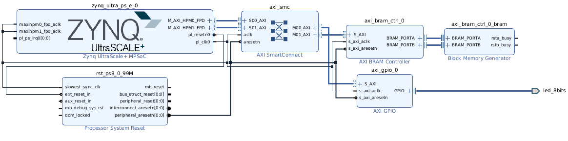
ZCU106 Configurable Example Design (CED) base block design.
PL Payload
Default Payload: VCU Extensible Platform
VCU Components:
H.264/H.265 encoder (4Kp60)
H.264/H.265 decoder (4Kp60)
Multi-stream support (8x 1080p30)
Low latency mode support
Video I/O:
HDMI 2.0 RX (up to 4Kp60)
HDMI 2.0 TX (up to 4Kp60)
SDI support through FMC card
MIPI CSI-2 support through FMC
Memory Infrastructure:
Frame buffers in PL DDR4
DMA engines for video data
Memory controller optimization
Additional Payloads Available:
PS Specifications
Processing System Configuration:
ZCU106 PS Peripheral Mappings in the CED
Peripheral |
MIO Pins |
Function |
|---|---|---|
SD1 |
MIO39-51 |
SD Card boot/storage |
USB0 |
MIO52-63 |
USB 3.0 host/device |
GEM3 |
MIO64-77 |
Gigabit Ethernet |
UART0 |
MIO18-19 |
Console UART |
UART1 |
MIO20-21 |
Debug UART |
I2C0 |
MIO14-15 |
I2C bus 0 (HDMI) |
I2C1 |
MIO16-17 |
I2C bus 1 (SFP+) |
GPIO |
MIO0-13, 22-37 |
General purpose I/O |
DP |
MIO27-30 |
DisplayPort AUX |
Interrupts
PS Interrupt Controller (GIC-400):
IRQ Range |
Source |
Count |
|---|---|---|
0-15 |
SGI |
16 |
16-31 |
PPI |
16 |
32-95 |
SPI |
64 |
121-136 |
16 |
VCU-Specific Interrupts:
IRQ |
Source |
Description |
|---|---|---|
104 |
VCU_ENC |
VCU encoder interrupt |
105 |
VCU_DEC |
VCU decoder interrupt |
106 |
VCU_MCU |
VCU MCU interrupt |
PS-PL Interrupts
PL to PS Interrupt Allocation:
Interrupt |
Source |
Usage |
|---|---|---|
PL[0] |
AXI INTC |
Aggregated PL interrupts |
PL[1] |
HDMI RX |
HDMI receive events |
PL[2] |
HDMI TX |
HDMI transmit events |
PL[3] |
10GbE |
10G Ethernet |
PL[4] |
V_FRMBUF_WR |
Frame buffer write complete |
PL[5] |
V_FR |
VPK180
Boot Firmware and Linux Disk Images
Linux Disk Image - Common Disk Image With Support for This Board
Refer to Common Specifications
Advanced Embedded Software Configurations Included
Xen Dom0 (through
edf-platform-disk-image; see image-variant comparison)The platform image installs the Linux OpenAMP runtime packages but does not ship a prebuilt VPK180 RPU firmware example for Linux to load with
remoteproc. Skip OpenAMP demo steps that load an RPU firmware ELF on the VPK180 platform image, or build and install the firmware yourself first.xen-zephyr-domu-imageZephyr DomU payload to follow in EDF 26.2
DDR Memory Map
The four DDR controllers (C0 - C3) each map their per-channel windows into the same shared LPDDR4 address regions. Access is interleaved across controllers by the NoC.
Start Address |
End Address |
Size |
Description |
Interface |
Access Type |
|---|---|---|---|---|---|
0x0000_0000_0000 |
0x0007_FFFF_FFFF |
2 GB |
C0_DDR_LOW0 |
NoC_lpddr0/S00_INI |
R/W |
0x0008_0000_0000 |
0x000F_FFFF_FFFF |
2 GB |
C0_DDR_LOW1 |
NoC_lpddr0/S00_INI |
R/W |
0x0500_0000_0000 |
0x0500_FFFF_FFFF |
4 GB |
C0_DDR_CH1 |
NoC_lpddr1/S00_INI |
R/W |
0x0600_0000_0000 |
0x0600_FFFF_FFFF |
4 GB |
C0_DDR_CH2 |
NoC_lpddr2/S00_INI |
R/W |
0x0500_0000_0000 |
0x0500_FFFF_FFFF |
4 GB |
C1_DDR_CH1 |
NoC_lpddr1/S01_INI |
R/W |
0x0600_0000_0000 |
0x0600_FFFF_FFFF |
4 GB |
C1_DDR_CH2 |
NoC_lpddr2/S01_INI |
R/W |
0x0500_0000_0000 |
0x0500_FFFF_FFFF |
4 GB |
C2_DDR_CH1 |
NoC_lpddr0/S02_INI |
R/W |
0x0600_0000_0000 |
0x0600_FFFF_FFFF |
4 GB |
C2_DDR_CH2 |
NoC_lpddr0/S02_INI |
R/W |
0x0500_0000_0000 |
0x0500_FFFF_FFFF |
4 GB |
C3_DDR_CH1 |
NoC_lpddr0/S03_INI |
R/W |
0x0600_0000_0000 |
0x0600_FFFF_FFFF |
4 GB |
C3_DDR_CH2 |
NoC_lpddr0/S03_INI |
R/W |
The DDR configuration is summarized as follows:
Total DDR: Multiple LPDDR4 component memories
Channel Configuration: 3 memory controllers, multiple channels
Memory Type: LPDDR4
Access: Through NoC (Network on Chip)
System Level Memory Map
Start Address |
Description |
Size |
Type |
|---|---|---|---|
0x0000_0000_0000 |
DDR Low Memory Region 0 |
2 GB |
DDR |
0x0008_0000_0000 |
DDR Low Memory Region 1 |
2 GB |
DDR |
0x0500_0000_0000 |
DDR Channel 1 (All Controllers) |
4 GB |
DDR |
0x0600_0000_0000 |
DDR Channel 2 (All Controllers) |
4 GB |
DDR |
0xA400_0000 |
AXI Block RAM Controller |
8 KB |
|
0xA401_0000 |
AXI GPIO 0 (LEDs) |
64 KB |
PL Peripheral |
0xA402_0000 |
AXI GPIO 1 (Push Buttons) |
64 KB |
PL Peripheral |
0xA403_0000 |
AXI GPIO 2 (DIP Switches) |
64 KB |
PL Peripheral |
0xF000_0000 |
CIPS Configuration Space |
PS Registers |
|
0xF100_0000 |
FPD Peripherals |
PS Peripherals |
|
0xF900_0000 |
LPD Peripherals |
PS Peripherals |
|
0xFE00_0000 |
PMC Peripherals |
||
0xFF00_0000 |
CPM / PCIe |
CPM |
Programmable Logic Peripheral Details
The following table provides a focused PL-peripheral view and repeats the same BRAM and GPIO base addresses listed in the preceding system memory map.
Base Address |
Peripheral |
Description |
Size |
|---|---|---|---|
0xA400_0000 |
BRAM storage |
8 KB |
|
0xA401_0000 |
GPIO_0 |
LED control (gpio_led) |
64 KB |
0xA402_0000 |
GPIO_1 |
Push buttons (gpio_pb) |
64 KB |
0xA403_0000 |
GPIO_2 |
DIP switches (gpio_dp) |
64 KB |
Quad SPI Memory Map
Default VPK180 QSPI memory map:
Start Address |
Description |
Size (MB) |
Start Sector |
R or R/W |
MTD |
MultiBoot Offset |
|---|---|---|---|---|---|---|
0x0000_0000 |
Boot Header |
1 |
0 |
R |
mtd0 |
0x0000 |
0x0010_0000 |
PLM Firmware |
2 |
16 |
R |
mtd1 |
|
0x0030_0000 |
2 |
48 |
R |
mtd2 |
||
0x0050_0000 |
Device Image (PDI) |
32 |
80 |
R |
mtd3 |
|
0x0250_0000 |
APU Application |
64 |
592 |
R |
mtd4 |
|
0x0650_0000 |
Linux Kernel |
32 |
1616 |
R |
mtd5 |
|
0x0850_0000 |
Device Tree |
1 |
2128 |
R |
mtd6 |
|
0x0860_0000 |
RootFS |
128 |
2144 |
R |
mtd7 |
|
0x1060_0000 |
User Data |
64 |
4192 |
R/W |
mtd8 |
|
0x1460_0000 |
Recovery Image |
32 |
5216 |
R |
mtd9 |
0x1460_0000 |
The QSPI controller is configured as follows:
Interface: PMC QSPI controller
Mode: Quad I/O (x4)
Boot Device: Primary boot source
Typical Size: 512 MB or 1 GB
Sector Size: 64 KB
Programming Secondary Boot Media
See Discovery and Evaluation
for writing the EDF Linux disk image (.wic) to an SD card.
Basic Board Interfaces
The board’s key interfaces, taken from the VPK180 block diagram, are grouped by function as follows:
- Memory
LPDDR4 component memory (3 controllers)
- High-Speed I/O
- Storage
SD 3.0 card interface
QSPI flash
- USB
USB 2.0 ULPI interface
- Networking
GEM (Gigabit Ethernet media access controller)
- Debug
JTAG interface
Mictor debug connector
- Expansion
FMC+ connector
GPIO headers
- Timing & Clocks
IEEE-1588 clock
SMA clock connectors
Powering the Board
The VPK180 main power input is:
Main Power Input: 12 V DC
The board’s power domains are:
Power sequencing is:
Controlled by system controller / PMC
Power indicators are:
Power-good LEDs
Default Boot Switch Settings
Boot Mode |
MODE[3:0] |
DIP Switch |
Description |
|---|---|---|---|
0000 |
SW1: OFF-OFF-OFF-OFF |
JTAG boot |
|
QSPI32 |
0010 |
SW1: OFF-OFF-ON-OFF |
QSPI boot |
SD1_LS |
1110 |
SW1: ON-ON-ON-OFF |
SD card boot |
USB |
0111 |
SW1: OFF-ON-ON-ON |
USB boot |
Note
Boot mode settings and switch numbering follow the VPK180 board user guide (UG1551).
System Controller Firmware Update
See the System Controller Updates Wiki page for more information.
Serial Console Connections Through USB Adapter
UART Channel |
Source |
Destination |
Purpose |
Default Settings |
|---|---|---|---|---|
UART0 |
PS MIO |
FTDI CH A |
Linux/APU Console |
115200,8,N,1 |
UART1 |
PMC MIO |
FTDI CH B |
PMC/PLM Console |
115200,8,N,1 |
UART2 |
EMIO |
FTDI CH C |
115200,8,N,1 |
|
UART3 |
FTDI CH D |
Spare / User |
115200,8,N,1 |
Base Vivado Design - Board Support Package and PS Specifications
This specification inherits from the common and device specific specifications, but also has evaluation board specific items. See also the following:
See Common Specifications for the embedded common platform Configurable Example Design (CED).
See Common Specifications for the Processing System (PS) common minimum specification.
PL Board I/O
Programmable Logic Input and Output Interfaces
Interface |
Type |
Location |
Description |
|---|---|---|---|
FMC+ Connector |
High-speed expansion |
PL banks |
FMC+ HPC compatible |
GPIO Headers |
Digital I/O |
PL banks |
General purpose |
EMIO Signals |
PS-PL interface |
XPIO |
Extended MIO |
Mictor Connector |
Debug |
PL banks |
High-speed |
SMA Connectors |
Clock / RF |
PL banks |
External clocks |
High-speed serial |
Dedicated |
Optical / FMC |
Programmable Logic Peripherals in Configurable Example Design
Controller |
Base Address |
Description |
Direction |
|---|---|---|---|
axi_gpio_0 |
0xA401_0000 |
GPIO LEDs |
Output |
axi_gpio_1 |
0xA402_0000 |
GPIO Push Buttons |
Input |
axi_gpio_2 |
0xA403_0000 |
GPIO DIP Switches |
Input |
axi_bram_ctrl_0 |
0xA400_0000 |
BRAM Controller |
Bidirectional |
Memory Map Interface Configuration
Memory Map Interface Clocks
Reference Programmable Logic Payload Information
See the Discovery and Evaluation
Enabling Secure Mode Flag in Boot Arguments
The versal_sysmon.secure_mode=1 kernel command-line flag enforces
secure access control on the Versal SYSMON interface. Enable
it for platform validation, secure production images, and environments
where System Monitor interfaces must follow secure-mode restrictions.
By default, versal_sysmon.secure_mode=1 is not enabled in
built images. To enable it, use the kernel command-line modification
workflow described in Setting Kernel Boot Arguments.
After the build completes, apply the flag by modifying
loader/entries/edf-linux.conf in the .wic image using
wic cp (extract, edit, and copy back).
Append the following argument to
the options line of edf-linux.conf:
versal_sysmon.secure_mode=1
After flashing the updated .wic image and booting the board,
verify the flag is active:
amd-edf:/home/amd-edf# cat /proc/cmdline
... versal_sysmon.secure_mode=1 ...
amd-edf:/home/amd-edf# dmesg | grep -i sysmon
# Example output (the exact driver message may vary by kernel version):
versal-sysmon ...: secure mode enabled
On other Versal boards that require the same flag, use the same workflow with that board’s image artifact name.